EQ public doc (PDF)
File information
This PDF 1.7 document has been generated by Adobe InDesign CS5.5 (7.5.1) / Adobe PDF Library 9.9, and has been sent on pdf-archive.com on 12/10/2011 at 20:18, from IP address 188.142.x.x.
The current document download page has been viewed 9249 times.
File size: 2.55 MB (15 pages).
Privacy: public file


File preview
Modular UREI 545 and 546
EQ clone and variations project
Schematics and Bill of
Materials for Parametric EQ
project
3 -
Modular parametric EQ project based on UREI 545 and 546
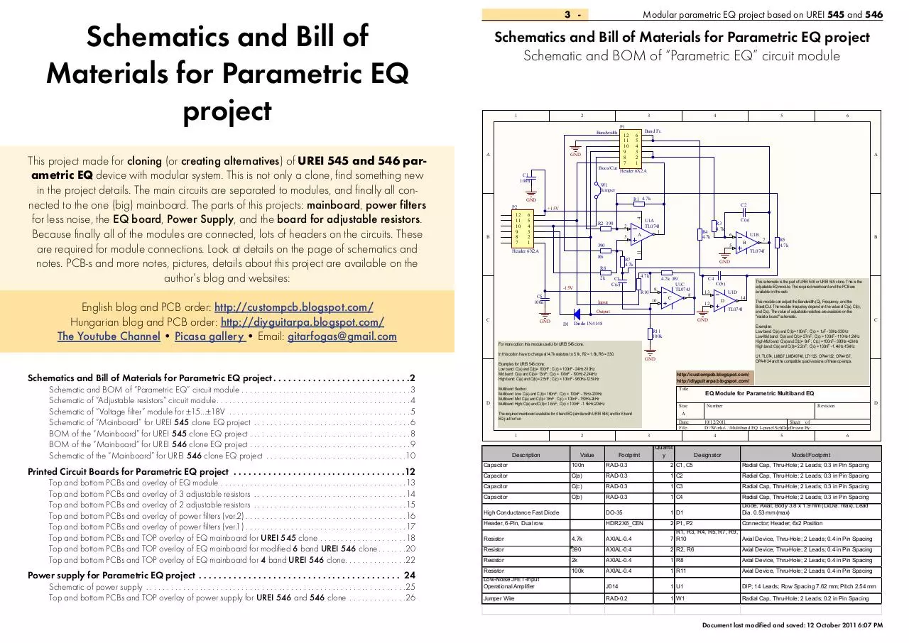
Schematics and Bill of Materials for Parametric EQ project
Schematic and BOM of “Parametric EQ” circuit module
1
2
3
Bandwidth
GND
A
Boos/Cut
C1
100n
B
Band Fr.
6
5
4
3
2
1
A
Header 6X2A
R1 4.7k
GND
P2
6
5
4
3
2
1
R2 390
2
3
A
Header 6X2A
Top and bottom PCBs and overlay of EQ module . . . . . . . . . . . . . . . . . . . . . . . . . . . . . . . . . . . . . . . . . . . . . 13
Top and bottom PCBs and overlay of 3 adjustable resistors . . . . . . . . . . . . . . . . . . . . . . . . . . . . . . . . . . . . . 14
Top and bottom PCBs and overlay of 2 adjustable resistors . . . . . . . . . . . . . . . . . . . . . . . . . . . . . . . . . . . . . 15
Top and bottom PCBs and overlay of power filters (ver.2) . . . . . . . . . . . . . . . . . . . . . . . . . . . . . . . . . . . . . . 16
Top and bottom PCBs and overlay of power filters (ver.1) . . . . . . . . . . . . . . . . . . . . . . . . . . . . . . . . . . . . . . 17
Top and bottom PCBs and TOP overlay of EQ mainboard for UREI 545 clone . . . . . . . . . . . . . . . . . . . . . 18
Top and bottom PCBs and TOP overlay of EQ mainboard for modified 6 band UREI 546 clone . . . . . . 20
Top and bottom PCBs and TOP overlay of EQ mainboard for 4 band UREI 546 clone . . . . . . . . . . . . . . 22
Power supply for Parametric EQ project . . . . . . . . . . . . . . . . . . . . . . . . . . . . . . . . . . . . . . . . . . 24
Schematic of power supply . . . . . . . . . . . . . . . . . . . . . . . . . . . . . . . . . . . . . . . . . . . . . . . . . . . . . . . . . . . . . . . 25
Top and bottom PCBs and TOP overlay of power supply for UREI 546 and 546 clone . . . . . . . . . . . . . . 26
R4
4.7k
R3
4.7k
R6
R7
4.7k
2k
C5
100n
GND
U1B
6
B
C3
C(c)
Input
TL074J
4.7k
4.7k R9
U1C
TL074J
9
R10
8
C
10
C4
U1D
13
D
12
14
TL074J
GND
D1 Diode 1N4148
http://custompcb.blogspot.com/
http://diyguitarpa.blogspot.com/
Multiband Section:
Multiband Low: C(a) and C(b)= 160nF ; C(c) = 100nF - 15Hz-200Hz
Multiband Mid: C(a) and C(b)= 16nF ; C(c) = 100nF - 150Hz-2kHz
Multiband High: C(a) and C(b)= 1.6nF ; C(c) = 100nF - 1.5kHz-20kHz
Title
Size
The required mainboard available for 4 band EQ (similar with UREI 546) and for 6 band
EQ just for fun.
2
Description
C
U1: TL074, LM837, LME49740, LT1125, OPA4132, OPA4137,
OPA4134 and the compatible quad versions of these op-amps.
GND
Examples for UREI 545 clone:
Low band: C(a) and C(b)= 100nF ; C(c) = 100nF - 24Hz-310Hz
Mid band: C(a) and C(b)= 13nF ; C(c) = 100nF - 190Hz-2.24kHz
High band: C(a) and C(b)= 2.5nF ; C(c) = 100nF - 960Hz-12.5kHz
This module can adjust the Bandwidth (Q), Frequency, and the
Boost/Cut. The module frequency depend on the value of C(a), C(b),
and C(c). The value of adjustable resistors are available on the
"resistor board" schematic.
Examples:
Low band: C(a) and C(b)= 100nF ; C(c) = 1uF - 30Hz-330Hz
Low-Mid band: C(a) and C(b)= 27nF ; C(c) = 100nF - 110Hz-1.2kHz
High-Mid band: C(a) and C(b)= 8nF ; C(c) = 100nF - 390Hz-4.2kHz
High band: C(a) and C(b)= 2.2nF ; C(c) = 100nF - 1.4kHz-15kHz
For more option, this module useful for UREI 545 clone.
1
B
R5
4.7k
This schematic is the part of UREI 546 or UREI 545 clone. This is the
adjustable EQ module. The required mainboard and the PCB are
available on the web.
C(b)
R11
100k
D
7
GND
Output
C
C(a)
5
R8
Schematics and Bill of Materials for Parametric EQ project . . . . . . . . . . . . . . . . . . . . . . . . . . . 2
Printed Circuit Boards for Parametric EQ project . . . . . . . . . . . . . . . . . . . . . . . . . . . . . . . . . . . 12
U1A
TL074J
1
390
In this option have to change all 4.7k resistors to 5.1k, R2 = 1.6k, R6 = 330,
Schematic and BOM of “Parametric EQ” circuit module . . . . . . . . . . . . . . . . . . . . . . . . . . . . . . . . . . . . . . . . . 3
Schematic of “Adjustable resistors” circuit module . . . . . . . . . . . . . . . . . . . . . . . . . . . . . . . . . . . . . . . . . . . . . . 4
Schematic of “Voltage filter” module for ±15...±18V . . . . . . . . . . . . . . . . . . . . . . . . . . . . . . . . . . . . . . . . . . . . 5
Schematic of “Mainboard” for UREI 545 clone EQ project . . . . . . . . . . . . . . . . . . . . . . . . . . . . . . . . . . . . . . 6
BOM of the “Mainboard” for UREI 545 clone EQ project . . . . . . . . . . . . . . . . . . . . . . . . . . . . . . . . . . . . . . 8
BOM of the “Mainboard” for UREI 546 clone EQ project . . . . . . . . . . . . . . . . . . . . . . . . . . . . . . . . . . . . . . 9
Schematic of the “Mainboard” for UREI 546 clone EQ project . . . . . . . . . . . . . . . . . . . . . . . . . . . . . . . . . . 10
C2
+15V
4
12
11
10
9
8
7
6
W1
Jumper
-15V
English blog and PCB order: http://custompcb.blogspot.com/
Hungarian blog and PCB order: http://diyguitarpa.blogspot.com/
The Youtube Channel • Picasa gallery • Email: gitarfogas@gmail.com
12
11
10
9
8
7
5
11
This project made for cloning (or creating alternatives) of UREI 545 and 546 parametric EQ device with modular system. This is not only a clone, find something new
in the project details. The main circuits are separated to modules, and finally all connected to the one (big) mainboard. The parts of this projects: mainboard, power filters
for less noise, the EQ board, Power Supply, and the board for adjustable resistors.
Because finally all of the modules are connected, lots of headers on the circuits. These
are required for module connections. Look at details on the page of schematics and
notes. PCB-s and more notes, pictures, details about this project are available on the
author’s blog and websites:
P1
4
Footprint
Number
D
Revision
A
Date:
File:
3
Value
EQ Module for Parametric Multiband EQ
10/12/2011
Sheet of
D:\!Works\..\Multiband EQ 1-panel.SchDocDrawn By:
4
Quantit
y
Designator
5
6
Model:Footprint
Capacitor
100n
RAD-0.3
2 C1, C5
Radial Cap, Thru-Hole; 2 Leads; 0.3 in Pin Spacing
Capacitor
C(a)
RAD-0.3
1 C2
Radial Cap, Thru-Hole; 2 Leads; 0.3 in Pin Spacing
Capacitor
C(c)
RAD-0.3
1 C3
Radial Cap, Thru-Hole; 2 Leads; 0.3 in Pin Spacing
Capacitor
C(b)
RAD-0.3
1 C4
High Conductance Fast Diode
DO-35
1 D1
Radial Cap, Thru-Hole; 2 Leads; 0.3 in Pin Spacing
Diode, Axial; Body 3.8 x 1.9 mm (LxDia. max), Lead
Dia. 0.53 mm (max)
Header, 6-Pin, Dual row
HDR2X6_CEN
Resistor
4.7k
AXIAL-0.4
2 P1, P2
Connector; Header; 6x2 Position
R1, R3, R4, R5, R7, R9,
7 R10
Axial Device, Thru-Hole; 2 Leads; 0.4 in Pin Spacing
Resistor
390
AXIAL-0.4
2 R2, R6
Axial Device, Thru-Hole; 2 Leads; 0.4 in Pin Spacing
Resistor
2k
AXIAL-0.4
1 R8
Axial Device, Thru-Hole; 2 Leads; 0.4 in Pin Spacing
Resistor
Low-Noise JFET-Input
Operational Amplifier
100k
AXIAL-0.4
1 R11
Axial Device, Thru-Hole; 2 Leads; 0.4 in Pin Spacing
J014
1 U1
DIP; 14 Leads; Row Spacing 7.62 mm; Pitch 2.54 mm
RAD-0.2
1 W1
Radial Cap, Thru-Hole; 2 Leads; 0.2 in Pin Spacing
Jumper Wire
Document last modified and saved: 12 October 2011 6:07 PM
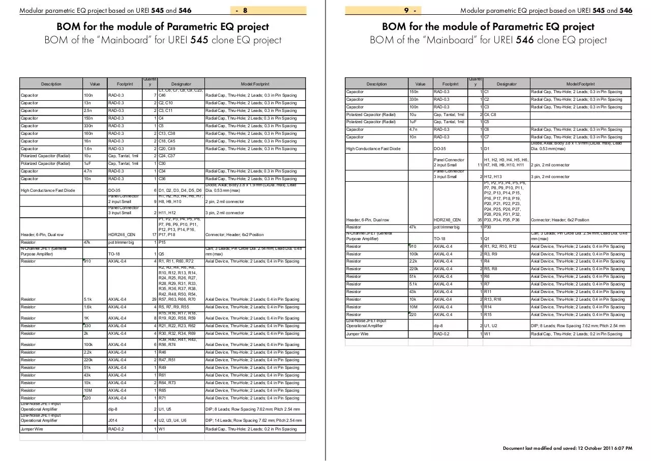
Modular parametric EQ project based on UREI 545 and 546
- 4
5 -
Schematic and BOM for the module of Parametric EQ project
Schematic of “Adjustable resistors” circuit module
1
2
3
5
P5
R (Band frequency)
A
4
1
2
3
4
5
6
P1
Pot stereo
Schematic and BOM for the module of Parametric EQ project.
Schematic of “Voltage filter” module for ±15...±18V
6
1
R (Bandwidth - Q)
7
8
9
10
11
12
Modular parametric EQ project based on UREI 545 and 546
2
3
4
5
6
A
A
A
P2
Pot stereo
P1
1
2
3
4
5
6
B
Header 6X2A
GND
C1
47uF 60V
7
8
9
10
11
12
R1
BC560C
Q1
C4
10uF C5
10uF
C3
100nF
12K
C8
47nF
GND
GND
GND
C2
100nF
BC550C
Q2
R2
12K
C6
47nF
47uF 60V
C7
B
GND
Header 6X2A
C
C
Title
P3
R (Boost/Cut)
1
2
3
4
5
6
P4
Pot stereo
B
This schematic is the part ofparametric EQ
projects. These projects are clones ofUREI
545 and 546 EQ-s. The value ofadjusteble
resistors are depending on the function ofEQ
module. This module required the mainboard
made for UREI545 or 546 clones.
7
8
9
10
11
12
http://custompcb.blogspot.com/
http://diyguitarpa.blogspot.com/
B
Description
Polarized Capacitor (Radial)
Value
47uF 60V
C
Date:
File:
3
Footprint
Elco 6mm, 1 mil
pins
Revision
10/11/2011
D:\!Works\..\PowerFilter.SchDoc
4
Quantit
y
Sheet of
Drawn By:
5
Designator
D
6
Model:Footprint
2 C1, C7
Capacitor
100nF
RAD-0.3
2 C2, C3
Polarized Capacitor (Radial)
10uF
Cap, Tantal, 1mil
2 C4, C5
Capacitor
47nF
RAD-0.3
2 C6, C8
Capacitor; 2 Leads
HDR2X6_CEN
1 P1
Header, 6-Pin, Dual row
Resistor values for UREI545 clone:
- Low cut and high cut: 50k stereo (P4)
- Bandwidth (Q): 10k mono (P2)
- Frequency: 10k stereo (P1)
- Boost/Cut: 10k mono (P4)
C
2
Number
A
This schematic is the partof preamps and EQ projects. This module filtering the symmatrical (+-) power for
circuits. PCB and another modules, mainboards are available.
1
Resistor values for UREI546 clone:
- Low cut and high cut: 55k stereo (P4)
- Bandwidth (Q): 10k mono (P2)
- Frequency: 55k stereo (P1)
- Boost/Cut: 10k mono (P4)
Header 6X2A
D
Size
Power filter module
Capacitor; 2 Leads
Transistor PNP Silicon
BC560C
29-04
1 Q1
Transistor NPN Silicon
BC550C
29-04
1 Q2
Connector; Header; 6x2 Position
TO, Flat Index; 3 In-Line, Axial Leads; Body Dia.
4.8mm; Leads 0.48 x 0.5 mm (max)
TO, Flat Index; 3 In-Line, Axial Leads; Body Dia.
4.8mm; Leads 0.48 x 0.5 mm (max)
Resistor
12K
AXIAL-0.4
2 R1, R2
Resistor; 2 Leads
For both:
Output module gain: 5k mono (P4)
http://custompcb.blogspot.com/
http://diyguitarpa.blogspot.com/
Title
Potmeter module for parametric EQ project
Size
D
Revision
D
A
Date:
File:
1
Description
Resistor
Resistor
Header, 6-Pin, Dual row
Resistor
Number
10/12/2011
D:\!Works\..\Pots.SchDoc
2
Value
R (Band
frequency)
R
(Bandwidth Q)
Sheet of
Drawn By:
3
Footprint
Pots Plastic
Stereo
4
Quantit
y
6
Model:Footprint
1 P1
Pots Plastic
Stereo
1 P2
HDR2X6_CEN
2 P3, P5
R (Boost/Cut)Pots Plastic Stereo
Designator
5
1 P4
Connector; Header; 6x2 Position
Notes
The 3th module required for the EQ mainboard is the power filter circuit. I like to use this simple
circuit to filter the problems of power. These circuits have to be connected to the headers P26-P29,
and P33-36 on the PCB of 546 clone mainboard. 8 (ot the PCB-V4 6) modules required for better
power and less noise, but if you think this is not important, you can wire pin 8 to pin 10 and pin
7 to pin 12 to ignore these circuits and boards.
We have two versions of power filter PCB. No difference between schematics, the one of them is
landscape, the another one is portrait orientation.
Document last modified and saved: 12 October 2011 6:07 PM
Modular parametric EQ project based on UREI 545 and 546
- 6
7 -
Modular parametric EQ project based on UREI 545 and 546
Schematic for the module of Parametric EQ project
Schematic of “Mainboard” for UREI 545 clone EQ project
2
3
P1
7
8
9
10
11
12
Bandwidth
12
11
10
9
8
7
P4
Header 6X2A
1
2
3
4
5
6
Low cut Fr.
1
GND
4
6
5
4
3
2
1
P2
Bandwidth
Low band Fr.
12
11
10
9
8
7
GND
Header 6X2A
5
Mid band Fr.
6
5
4
3
2
1
6
P3
Bandwidth
Header 6X2A
12
11
10
9
8
7
High band Fr.
6
5
4
3
2
1
Header 6X2A
GND
R1
2
1
3
C4
150n
R5 1.6k
U2A
2
3
TL074J
330
R21
H3
GND GND
1
A
100n
R6
5.1k
B
R36
5.1k
7
R31
5.1k
H4
U2C
8
C
10
P7
C9
5.1k R27
9
TL074J
R39
13
P5
D
12
TL074J
14
U2D
GND
U3A
TL074J
1
GND GND
R8
5.1k
R32
2k
6
5
4
3
2
1
R25
5.1k
13n
R9 1.6k
U3B
6
B
TL074J
C7
100n
R33
5.1k
C10
13n
5.1k R28
U3C
TL074J
8
C
9
10
U3D
13
D
12
R40
P6
14
TL074J
GND
100n
1.6n
2
1
5.1k
TL074J
U6B
6
B
5
R63
5.1k
9
R57
5.1k
13
D
12
TL074J
P11
7
8
9
10
11
12
C49
1.6n
4
R56
100k
R60
910
GND
R74
100k
TL074J
GND
14
Bandwidth
GND
P8
Header 6X2A
12
11
10
9
8
7
6
5
4
3
2
1
D5
Diode 1N4148
R61
43k
D6
GND
R72
910
R73
10k
Multiband Fr.
R49
51k
220k
R64
10k
P10
Header 6X2A
C37
10u
GND
P15
Pot Trimmer
47k
GND
W1
C24
10u
D
R38
5.1k
TL074J
GND
+15V Stage4
Q5
2N3370
3
R65
10M
GND
+15V Stage6
-15V Stage6
Jumper
GND
220
P9
12
11
10
9
8
7
P13
Header 6X2A
GND
R71
GND
P12
Header 6X2A
C
GND
6
5
4
3
2
1
+15V Stage5
-15V Stage5
P14
Header 6X2A
Output Gain
Header 6X2A
Header 6X2A
P16
Header 6X2A
GND
+15V Stage1
-15V Stage1
1
GND
H11
3
GND GND
+15V Stage2
-15V Stage2
Low band: C(a) and C(b)= 100nF ; C(c) = 100nF - 24Hz-310Hz
Mid band: C(a) and C(b)= 13nF ; C(c) = 100nF - 190Hz-2.24kHz
High band: C(a) and C(b)= 2.5nF ; C(c) = 100nF - 960Hz-12.5kHz
P17
Header 6X2A
7
8
9
10
11
12
This EQ can adjust the bandwidth (Q), Frequency, and the Boost/Cut.
GND
Multiband Section:
Multiband Low: C(a) and C(b)= 160nF ; C(c) = 100nF - 15Hz-200Hz
Multiband Mid: C(a) and C(b)= 16nF ; C(c) = 100nF - 150Hz-2kHz
Multiband High: C(a) and C(b)= 1.6nF ; C(c) = 100nF - 1.5kHz-20kHz
Ux: TL074, LM837, LME49740, LT1125, OPA4132, OPA4137, OPA4134 and the dual versions of these op-amps.
2
P18
Header 6X2A
1
2
3
4
5
6
2
This schematic is the part of UREI 545 clone. This is the mainboard. The required additional potmeter-modules, power filter moadules and the PCB are available.
7
8
9
10
11
12
R59
1K
GND
1
2
3
4
5
6
R58
1K
3
D
B
R50
5.1k
GND
Diode 1N4148
C36
10n
1
A
GND
U6D
8
C
12
TL074J
14
-15V Stage3
R46
2.2k
TL072P
C23
R51
100n
D4
4.7n
C34
Diode 1N4148
5.1k R66
U6C
10
1
2
3
4
5
6
16n
R47
220k
Diode 1N4148
C30 1uF
GND
R70
5.1k
U4D
13
8
H6
U5A
3
D3
6
5
4
3
2
1
C
160n
C45
Diode 1N4148
7
B
5
1
2
12
11
10
9
8
7
R69 C46
2k 100n
6
2
R43
100k
Diode 1N4148
D2
U5B
TL072P
High cut Fr.
330
7
C38
TL074J
11
R62
D1
7
8
9
10
11
12
R54
C
1
2
3
4
5
6
1
A
U4C
-15V Stage4
7
8
9
10
11
12
C20
4
3
C11
2.5n
5.1k R29
9
1
2
3
4
5
6
16n
5.1k
1.6k
R35
5.1k
2
C18
1
H10
U6A
7
TL074J
1
H9
8
160n
1
2
H8
1
2
C13
2
2
B
GND
R41
100k
+15V Stage3
Output
R48
R55
U4B
6
GND
5.1k
H7
2.5n
GND
R42
Multiband
R10
5.1k
5
10
Header 6X2A
B
R14
5.1k
R26
5.1k
C8
A
C3
R20
1K
GND GND
TL074J
Header 6X2A
100k
GND
R34
2k
6
5
4
3
2
1
1
A
330
R23
12
11
10
9
8
7
U4A
2
3
R37
5.1k
7
GND
Header 6X2A
100k
R13
5.1k
5
R22
12
11
10
9
8
7
A
3
TL074J
100n
2
330
GND
R30
2k 100n
6
5
4
3
2
1
R7 1.6k
U2B
6
5
R24
5.1k
C6
12
11
10
9
8
7
R12
5.1k
R19
1K
4
4
U1A
TL072P
1
5.1k
7
8
9
10
11
12
1
A
R4
C2
R18
1K
1
2
3
4
5
6
2
2
GND
4
1
C5
7
B
5
R11
910
R17
1K
5.1k
7
8
9
10
11
12
330n
U1B
TL072P
R3
C1
1
2
3
4
5
6
6
R16
1K
11
In
H2
R15
1K
5.1k
8
H1
2
R2
GND
4
910
1
11
2
11
A
GND
-15V
1
+15V
H12
Title
GND
UREI 545 Clone Mainboard
Size
http://custompcb.blogspot.com/
http://diyguitarpa.blogspot.com/
1
D
2
3
4
5
Number
Revision
Tabloid
Date:
File:
10/11/2011
Sheet of
D:\!Works\..\UREI545-EQ Pots PF-Panels.SchDoc
Drawn By:
6
Document last modified and saved: 12 October 2011 6:07 PM
Modular parametric EQ project based on UREI 545 and 546
- 8
9 -
BOM for the module of Parametric EQ project
BOM of the “Mainboard” for UREI 545 clone EQ project
Description
Value
Footprint
Capacitor
100n
RAD-0.3
Capacitor
13n
RAD-0.3
2 C2, C10
Radial Cap, Thru-Hole; 2 Leads; 0.3 in Pin Spacing
Capacitor
2.5n
RAD-0.3
2 C3, C11
Radial Cap, Thru-Hole; 2 Leads; 0.3 in Pin Spacing
Capacitor
150n
RAD-0.3
1 C4
Radial Cap, Thru-Hole; 2 Leads; 0.3 in Pin Spacing
Capacitor
330n
RAD-0.3
1 C5
Radial Cap, Thru-Hole; 2 Leads; 0.3 in Pin Spacing
Capacitor
160n
RAD-0.3
2 C13, C38
Radial Cap, Thru-Hole; 2 Leads; 0.3 in Pin Spacing
Capacitor
16n
RAD-0.3
2 C18, C45
Radial Cap, Thru-Hole; 2 Leads; 0.3 in Pin Spacing
Radial Cap, Thru-Hole; 2 Leads; 0.3 in Pin Spacing
Capacitor
1.6n
RAD-0.3
2 C20, C49
Polarized Capacitor (Radial)
10u
Cap, Tantal, 1mil
2 C24, C37
Polarized Capacitor (Radial)
1uF
Cap, Tantal, 1mil
1 C30
Capacitor
4.7n
RAD-0.3
1 C34
Capacitor
10n
RAD-0.3
1 C36
High Conductance Fast Diode
DO-35
Panel Connector
2 input Small
Panel Connector
3 input Small
Header, 6-Pin, Dual row
HDR2X6_CEN
Resistor
N-Channel JFET (General
Purpose Amplifier)
47k
Resistor
910
Description
2 H11, H12
P1, P2, P3, P4, P5, P6,
P7, P8, P9, P10, P11,
P12, P13, P14, P16,
17 P17, P18
1 P15
TO-18
1 Q5
Footprint
Model:Footprint
RAD-0.3
1 C1
Radial Cap, Thru-Hole; 2 Leads; 0.3 in Pin Spacing
Capacitor
330n
RAD-0.3
1 C2
Radial Cap, Thru-Hole; 2 Leads; 0.3 in Pin Spacing
Radial Cap, Thru-Hole; 2 Leads; 0.3 in Pin Spacing
Capacitor
100n
RAD-0.3
1 C3
Polarized Capacitor (Radial)
10u
Cap, Tantal, 1mil
2 C4, C8
Polarized Capacitor (Radial)
1uF
Cap, Tantal, 1mil
1 C5
Capacitor
4.7n
RAD-0.3
1 C6
Radial Cap, Thru-Hole; 2 Leads; 0.3 in Pin Spacing
Capacitor
10n
RAD-0.3
1 C7
DO-35
1 D1
Radial Cap, Thru-Hole; 2 Leads; 0.3 in Pin Spacing
Diode, Axial; Body 3.8 x 1.9 mm (LxDia. max), Lead
Dia. 0.53 mm (max)
High Conductance Fast Diode
Panel Connector
2 input Small
Panel Connector
3 input Small
3 pin, 2 mil connector
Header, 6-Pin, Dual row
Can; 3 Leads; Pin Circle Dia. 2.54 mm; Lead Dia. 0.48
mm (max)
Designator
150n
Radial Cap, Thru-Hole; 2 Leads; 0.3 in Pin Spacing
Connector; Header; 6x2 Position
Quantit
y
Capacitor
HDR2X6_CEN
H1, H2, H3, H4, H5, H6,
11 H7, H8, H9, H10, H11
2 pin, 2 mil connector
2 H12, H13
P1, P2, P3, P4, P5, P6,
P7, P8, P9, P10, P11,
P12, P13, P14, P15,
P16, P17, P18, P19,
P20, P21, P22, P23,
P24, P25, P26, P27,
P28, P29, P31, P32,
35 P33, P34, P35, P36
pot trimmer big
1 P30
TO-18
1 Q1
3 pin, 2 mil connector
Connector; Header; 6x2 Position
Resistor
N-Channel JFET (General
Purpose Amplifier)
47k
Resistor
910
AXIAL-0.4
4 R1, R2, R10, R12
Axial Device, Thru-Hole; 2 Leads; 0.4 in Pin Spacing
Resistor
100k
AXIAL-0.4
2 R3, R9
Axial Device, Thru-Hole; 2 Leads; 0.4 in Pin Spacing
Resistor
2.2k
AXIAL-0.4
1 R4
Axial Device, Thru-Hole; 2 Leads; 0.4 in Pin Spacing
Resistor
220k
AXIAL-0.4
2 R5, R8
Axial Device, Thru-Hole; 2 Leads; 0.4 in Pin Spacing
Resistor
51k
AXIAL-0.4
1 R6
Axial Device, Thru-Hole; 2 Leads; 0.4 in Pin Spacing
Resistor
5.1k
AXIAL-0.4
1 R7
Axial Device, Thru-Hole; 2 Leads; 0.4 in Pin Spacing
Resistor
43k
AXIAL-0.4
1 R11
Axial Device, Thru-Hole; 2 Leads; 0.4 in Pin Spacing
Can; 3 Leads; Pin Circle Dia. 2.54 mm; Lead Dia. 0.48
mm (max)
4 R1, R11, R60, R72
R2, R3, R4, R6, R8,
R10, R12, R13, R14,
R24, R25, R26, R27,
R28, R29, R31, R33,
R35, R36, R37, R38,
R42, R48, R50, R54,
29 R57, R63, R66, R70
Axial Device, Thru-Hole; 2 Leads; 0.4 in Pin Spacing
Axial Device, Thru-Hole; 2 Leads; 0.4 in Pin Spacing
Resistor
10k
AXIAL-0.4
2 R13, R16
Axial Device, Thru-Hole; 2 Leads; 0.4 in Pin Spacing
Axial Device, Thru-Hole; 2 Leads; 0.4 in Pin Spacing
Resistor
10M
AXIAL-0.4
1 R14
Axial Device, Thru-Hole; 2 Leads; 0.4 in Pin Spacing
Axial Device, Thru-Hole; 2 Leads; 0.4 in Pin Spacing
220
AXIAL-0.4
1 R15
Axial Device, Thru-Hole; 2 Leads; 0.4 in Pin Spacing
dip-8
2 U1, U2
DIP; 8 Leads; Row Spacing 7.62 mm; Pitch 2.54 mm
RAD-0.2
1 W1
Radial Cap, Thru-Hole; 2 Leads; 0.2 in Pin Spacing
Resistor
5.1k
AXIAL-0.4
Resistor
1.6k
AXIAL-0.4
Resistor
1K
AXIAL-0.4
4 R5, R7, R9, R55
R15, R16, R17, R18,
8 R19, R20, R58, R59
Resistor
330
AXIAL-0.4
4 R21, R22, R23, R62
Axial Device, Thru-Hole; 2 Leads; 0.4 in Pin Spacing
Resistor
Low-Noise JFET-Input
Operational Amplifier
Resistor
2k
AXIAL-0.4
Axial Device, Thru-Hole; 2 Leads; 0.4 in Pin Spacing
Jumper Wire
Resistor
100k
AXIAL-0.4
4 R30, R32, R34, R69
R39, R40, R41, R43,
6 R56, R74
Resistor
2.2k
AXIAL-0.4
1 R46
Axial Device, Thru-Hole; 2 Leads; 0.4 in Pin Spacing
Resistor
220k
AXIAL-0.4
2 R47, R51
Axial Device, Thru-Hole; 2 Leads; 0.4 in Pin Spacing
Resistor
51k
AXIAL-0.4
1 R49
Axial Device, Thru-Hole; 2 Leads; 0.4 in Pin Spacing
Resistor
43k
AXIAL-0.4
1 R61
Axial Device, Thru-Hole; 2 Leads; 0.4 in Pin Spacing
Resistor
10k
AXIAL-0.4
2 R64, R73
Axial Device, Thru-Hole; 2 Leads; 0.4 in Pin Spacing
Resistor
10M
AXIAL-0.4
1 R65
Axial Device, Thru-Hole; 2 Leads; 0.4 in Pin Spacing
Resistor
Low-Noise JFET-Input
Operational Amplifier
Low-Noise JFET-Input
Operational Amplifier
220
AXIAL-0.4
1 R71
Axial Device, Thru-Hole; 2 Leads; 0.4 in Pin Spacing
dip-8
2 U1, U5
DIP; 8 Leads; Row Spacing 7.62 mm; Pitch 2.54 mm
J014
4 U2, U3, U4, U6
DIP; 14 Leads; Row Spacing 7.62 mm; Pitch 2.54 mm
RAD-0.2
1 W1
Radial Cap, Thru-Hole; 2 Leads; 0.2 in Pin Spacing
Jumper Wire
Value
Radial Cap, Thru-Hole; 2 Leads; 0.3 in Pin Spacing
Diode, Axial; Body 3.8 x 1.9 mm (LxDia. max), Lead
6 D1, D2, D3, D4, D5, D6 Dia. 0.53 mm (max)
H1, H2, H3, H4, H6, H7,
9 H8, H9, H10
2 pin, 2 mil connector
pot trimmer big
AXIAL-0.4
BOM for the module of Parametric EQ project
BOM of the “Mainboard” for UREI 546 clone EQ project
Quantit
y
Designator
Model:Footprint
C1, C6, C7, C8, C9, C23,
7 C46
Radial Cap, Thru-Hole; 2 Leads; 0.3 in Pin Spacing
Modular parametric EQ project based on UREI 545 and 546
Axial Device, Thru-Hole; 2 Leads; 0.4 in Pin Spacing
Document last modified and saved: 12 October 2011 6:07 PM
Modular parametric EQ project based on UREI 545 and 546
- 10
11 -
Modular parametric EQ project based on UREI 545 and 546
Schematic for the module of Parametric EQ project
Schematic of the “Mainboard” for UREI 546 clone EQ project
1
2
Notes
This “mainboard” have large amount
of “headers” (connectors) because the
smallest modules connected and collected to this board.
3
P1
4
P2
1
2
3
4
5
6
7
8
9
10
11
12
1
2
3
4
5
6
5
P3
7
8
9
10
11
12
6
P4
1
2
3
4
5
6
7
8
9
10
11
12
1
2
3
4
5
6
P5
7
8
9
10
11
12
P6
1
2
3
4
5
6
7
8
9
10
11
12
1
2
3
4
5
6
7
8
9
10
11
12
Header 6X2A
Header 6X2A
Header 6X2A
Header 6X2A
Header 6X2A
Header 6X2A
P7
P8
P9
P10
P11
P12
1
2
3
4
5
6
P13
Header 6X2A
1
2
3
4
5
6
7
8
9
10
11
12
A
Low cut Fr.
A
7
8
9
10
11
12
1
2
3
4
5
6
7
8
9
10
11
12
1
2
3
4
5
6
7
8
9
10
11
12
1
2
3
4
5
6
7
8
9
10
11
12
1
2
3
4
5
6
7
8
9
10
11
12
1
2
3
4
5
6
7
8
9
10
11
12
Header 6X2A
Header 6X2A
Header 6X2A
Header 6X2A
Header 6X2A
Header 6X2A
P14
P15
P16
P17
P18
P19
R1
2
910
1
8
In
6
330n
C1
150n
2
3
A
Header 6X2A
7
8
9
10
11
12
Header 6X2A
GND
1
2
3
4
5
6
7
8
9
10
11
12
1
2
3
4
5
6
Header 6X2A
GND
7
8
9
10
11
12
1
2
3
4
5
6
Header 6X2A
GND
7
8
9
10
11
12
Header 6X2A
GND
1
2
3
4
5
6
7
8
9
10
11
12
Header 6X2A
GND
GND
Header 6X2A
H6
1
2
3
4
5
6
Header 6X2A
P23
7
8
9
10
11
12
1
2
3
4
5
6
Header 6X2A
-15V Stage 8
P24
7
8
9
10
11
12
1
2
3
4
5
6
Header 6X2A
1
2
3
4
5
6
Header 6X2A
H7
H8
P25
7
8
9
10
11
12
H9
+15v Stage 8
B
H10
+15V Stage5
Diode Bus
7
8
9
10
11
12
Header 6X2A
2
2
-15V Stage 7
P22
7
8
9
10
11
12
1
1
2
3
4
5
6
2
H5
7
8
9
10
11
12
1
P21
1
2
3
4
5
6
1
P20
H4
2
H3
1
1
GND
1
2
3
4
5
6
2
B
2
R2
910
7
8
9
10
11
12
1
1
7
1
2
5
C2
U1B
TL072P
2
1
H2
B
U1A
TL072P
1
4
2
1
2
3
4
5
6
GND
H1
P29
Header 6X2A
R12
910
1
2
3
4
5
6
7
8
9
10
11
12
10n
GND
R13
10k
GND
P32
Header 6X2A
12
11
10
9
8
7
6
5
4
3
2
1
R16
10k
High cut Fr.
GND
D1
Diode 1N4148
R11
43k
C7
R7
5.1k
7
8
9
10
11
12
R10
910
220k
GND
C4
10u
C8
10u
GND
P30
Pot Trimmer
47k
GND
W1
Jumper
GND
Q1
2N3370
3
R14
10M
P28
Header 6X2A
GND
C
+15V Stage6
-15V Stage6
R15
GND
P31
12
11
10
9
8
7
P27
Header 6X2A
1
2
3
4
5
6
GND
R6
51k
GND
220
GND
6
5
4
3
2
1
7
8
9
10
11
12
+15V Stage 7
100n
R9
100k
-15V Stage5
TL072P
C3
R8
P33
Header 6X2A
1
2
3
4
5
6
C5 1uF
4.7n
C6
-15V Stage3
7
8
9
10
11
12
R5
220k
1
A
1
2
3
4
5
6
3
7
8
9
10
11
12
7
B
+15V Stage3
R4
2.2k
P34
Header 6X2A
1
2
3
4
5
6
2
4
5
U2B
TL072P
H11
U2A
2
6
1
-15V Stage4
1
8
GND
C
2
R3
100k
1
2
3
4
5
6
7
8
9
10
11
12
+15V Stage4
Output
P26
Header 6X2A
Output Gain
Header 6X2A
GND
+15V Stage1
-15V Stage1
1
H12
D
P35
Header 6X2A
1
2
3
4
5
6
Examples:
Low band: C(a) and C(b)= 100nF ; C(c) = 1uF - 30Hz-330Hz
Low-Mid band: C(a) and C(b)= 27nF ; C(c) = 100nF - 110Hz-1.2kHz
High-Mid band: C(a) and C(b)= 8nF ; C(c) = 100nF - 390Hz-4.2kHz
High band: C(a) and C(b)= 2.2nF ; C(c) = 100nF - 1.4kHz-15kHz
7
8
9
10
11
12
2
+15V Stage2
-15V Stage2
P36
Header 6X2A
1
2
3
4
5
6
This EQ with additional EQ module can adjust the bandwidth (Q), Frequency, and the Boost/Cut.
7
8
9
10
11
12
This schematic is the part of EQ circuit based on UREI 546 clone. This is the mainboard. The required additional potmeter-modules, EQ modules, power filter modules and the PCB are available.
3
GND
GND
D
This module have 6 several EQ cards, but working with 4....6 modules depending on the required bands.
3
GND
2
-15V
1
+15V
H13
Title
GND
Size
http://custompcb.blogspot.com/
http://diyguitarpa.blogspot.com/
1
UREI 546 Clone Mainboard
2
3
4
5
Number
Revision
Tabloid
Date:
File:
10/11/2011
Sheet of
D:\!Works\..\UREI546-based MB-EQ.SchDoc
Drawn By:
The required most important modules are the EQ module. This panel
have to be connected to the headers
P14...P25. This is 12 connectors, but 6
modules only, because 1 EQ module
have 2 headers, look at the PCB of
EQ module.
Under these modules (on the PCB)
have 6 connectors for adjustable resistors. For the EQ modules required 3
resistors/module, adjusting the bandwidth, the frequency, and the cut/
boost, from P1 to P12. And required 3
smallest resistor modules with only one
header for low cut filter P13, high cut
filter P32, and to adjust the output
gain P31. Visit the PCB board about
adjustable resistors.
The 3th module required for this board
is the power filter board. I like to use
this simple circuit to filter the problem of
power. These circuits have to be connected to the headers P26-P29, and
P33-36. These are 8 modules for better
power and less noise, but if you think
this is not important, you can wire
pin 8 to pin 10 and pin 7 to pin 12 to
ignore these circuits and boards.
Finally in this schematic have connectors for 6 parametric EQ bands instead
of 4 (like in the original UREI 546). This
is just for fun, you can ignore the last 2
band and boards, but you can build 6
bands parametric EQ instead if 4 just
for fun.
6
Document last modified and saved: 12 October 2011 6:07 PM
Modular parametric EQ project based on UREI 545 and 546
- 12
13 -
Modular parametric EQ project based on UREI 545 and 546
PCB for the module of Parametric EQ project
Top and bottom PCBs and overlay of EQ module
TOP LAYER
BOTTOM LAYER
PCB OVERLAY
OVERLAY ON TOP LAYER
Printed Circuit Boards
for Parametric EQ
project
U1
C2
R9 R11
R5
C1
R2
R10
R3
C5
12
6
P1
7
1
7
1
12
6
P2
D1
R6
R5
R1
R4
12
6
R10
R7 R8
R1
R4
W1
C3
R6
P2
C1
W1
R2
R3
C5
7
1
D1
12
6
R7 R8
C2
C4
C4
C3
U1
P1
7
1
R9 R11
Document last modified and saved: 12 October 2011 6:07 PM
Modular parametric EQ project based on UREI 545 and 546
- 14
15 -
PCB for the module of Parametric EQ project
Top and bottom PCBs and overlay of 3 adjustable resistors
Modular parametric EQ project based on UREI 545 and 546
PCB for the module of Parametric EQ project
Top and bottom PCBs and overlay of 2 adjustable resistors
Notes
BOTTOM LAYER
TOP LAYER
BOTTOM LAYER
TOP LAYER
I made 2 versions
of PCB for adjustable resistors, because one of these
made for max. 2
(or 1 only) mono
and stereo adjustable resistors (for
high cut and low
cut filters, and for
output gain), the
another one is
made for max. 3
(or 2 or 1) resistors (adjust Freq.,
Boost, and Q features of EQ). The
bigger’s have 2
connectors,
the
smallest for 2 resistors have 1 connector only. Make
sure the board
direction is correct
before you finish it.
P2
P2
PCB OVERLAY
PCB OVERLAY
P2
P5
12
6
12
6
P3
7 12
1
6
7
1
7 12
1
6
P5
7
1
12
6
P3
P1
7
1
P4
P1
12
6
P4
OVERLAY ON TOP LAYER
P1
OVERLAY ON TOP LAYER
P1
P5
7
1
P2
P5
Document last modified and saved: 12 October 2011 6:07 PM
Modular parametric EQ project based on UREI 545 and 546
- 16
17 -
PCB for the module of Parametric EQ project
Top and bottom PCBs and overlay of power filters (ver.1)
TOP LAYER
BOTTOM LAYER
PCB for the module of Parametric EQ project
Top and bottom PCBs and overlay of power filters (ver.2)
Modular parametric EQ project based on UREI 545 and 546
TOP LAYER
Notes
We have two versions of power filter PCB. No
difference between schematics, the one of them is
landscape, the another one is portrait.
BOTTOM LAYER
OVERLAY ON TOP LAYER
C8
C4
3
1
C7
Q2
C6 C2
R2
P1
12
6
PCB OVERLAY
12
6
Q1
C1
R1
C4
C8
C3
C3 C8
12
6
3
1
C6
R1
P1
7
1
C5
C2
7
1
R2
C1
Q1
C1
3
1
R2
Q2
C7
C6
P1
7
1
C4
3
1
3
1
R2
C1
R1
C6 C2
3
1
C3
R1
3
1
C2
Q1
C7
Q2
3
1
Q1
Q2
C7
C5
C5
C5
C4
PCB OVERLAY
C3 C8
P1
7
1
12
6
OVERLAY ON TOP LAYER
Document last modified and saved: 12 October 2011 6:07 PM
Modular parametric EQ project based on UREI 545 and 546
- 18
19 -
Modular parametric EQ project based on UREI 545 and 546
PCB for the V.2 mainboard of Parametric EQ project
Top and bottom PCBs and TOP overlay of EQ mainboard for
UREI 545 clone
H12
H1
H2
H4
Q5
R51
2
3
R49
P15
U5
W1
C37
R8
R7
R65
R22
R6
R27 R21
D6 D5 D4
R33 R3
U2
R12 R39
C10
R2
R5
R28 R32
R30
R18
R16
C4
R17
R20
R15
R9
R34
R35
H7
R48R62 C13
H10
C45
R29
R23
H8
C18
C8
C7
R4
U1
R66R69 C20
U6
R57
C2
C5
R1 R11
R41 R38
U4
C34
R72
R40
R36
R24
TOP LAYER
R26
U3
C9
H6
R54 R70
C11
R10
R61
C3
R42
C46
R19
PCB TOP OVERLAY
C6
R14
R13 R25
R43
D2 D1
D3
C1
R31
R73
C23
C30
R37
R64
R60 R56
R47 R46 C36
R50
1
C24
H11
H3
R55
C38
H9
R63
C49
R74
R71 R59 R58
H12
H1
H2
H4
Q5
R60 R56
R47 R46 C36
R50
1
C24
H11
H3
2
3
R49
P15
U5
W1
C37
R8
R7
R65
R22
C30
R37
C1
R31
R27 R21
D6 D5 D4
R33 R3
U2
R12 R39
C10
R5
R28 R32
C9
BOTTOM LAYER
R30
R24
U1
C11
R10
R41 R38
U4
C4
R15
R54 R70
H6
U6
C18
R18
R20
R17
R29
R9
R34
R23
C45
C3
R42
C46
R35
R19
R55
C38
R63
R74
R71 R59 R58
H8
H7
R48R62 C13
C7
R4
C34
R66R69 C20
C8
R57
C2
R16
C23
R43
R72
R40
R36
C5
R1 R11
R26
U3
C6
R14
R13 R25
R61
C49
H10
H9
TOP OVERLAY ON TOP LAYER
R2
D2 D1
D3
R6
R73
R64
R51
Document last modified and saved: 12 October 2011 6:07 PM
Modular parametric EQ project based on UREI 545 and 546
PCB TOP OVERLAY
H5
W1
R1 R16P30
R15 R13 R14 R12
H3
H2
Q1
D1
3
PCB for the V.3 mainboard of Parametric EQ project
Top and bottom PCBs and TOP overlay of EQ mainboard for
modified 6 band UREI 546 clone
21 -
2
- 20
1
C7 R11 R10 R3
H12
H13
C8
C2 C1 R2 U1
C6
H11
R8 R6 R7
R9
C4
C5
R5 R4 U2
C3
H1
H6
H4
H8
H9
H7
H10
TOP LAYER
TOP OVERLAY ON TOP LAYER
R1 R16P30
R15 R13 R14 R12
H3
H2
Q1
D1
3
W1
1
H5
2
Modular parametric EQ project based on UREI 545 and 546
C7 R11 R10 R3
H12
H13
C8
C2 C1 R2 U1
H11
C6
R8 R6 R7
R9
C4
C5
R5 R4 U2
C3
H1
H4
H6
H9
H8
H7
H10
BOTTOM LAYER
Document last modified and saved: 12 October 2011 6:07 PM
Modular parametric EQ project based on UREI 545 and 546
- 22
23 -
PCB for the V.4 mainboard of Parametric EQ project
Top and bottom PCBs and TOP overlay of EQ mainboard for
4 band UREI 546 clone
Modular parametric EQ project based on UREI 545 and 546
PCB TOP OVERLAY
H1
H2
R16R9 R8 R6 R7
W1
H5
H3
R4
R5
H11
Q1
1
C3
P30
H13
H12
R15 R13R14R12
D1
U2
C7
R11R10 R3
3
2
H4
C8
H8
C4
H7
C5
H10
U1
TOP LAYER
C6 R1
C1 C2
R2
Notes
TOP OVERLAY ON TOP LAYER
H1
H2
R16R9 R8 R6 R7
W1
P30
BOTTOM LAYER
U1
C6 R1
C1 C2
R2
H3
H5
R4
R5
H11
Q1
1
C3
H4
H13
H12
R15 R13R14R12
D1
U2
3
2
C4
H8
C8
H7
C5
C7
R11R10 R3
This is the 3th variations of
UREI mainboards (but the
version number is 4 because
the first is not published).
H10
This mainboard have no
more than 4 bands (instead
of 6), Low, Low-mid, Highmid, and High. This 4 bands
are same than the bands of
original UREI 546 EQ. This
mainboard have 8 connectors for 4 adjustable bands
with 3 potentiometers required for 1 band, and one
potentiometer required for
low cut, high cut, and output
gain circuits. The benefit of
this board the smaller size,
and lower final costs.
Document last modified and saved: 12 October 2011 6:07 PM
Modular parametric EQ project based on UREI 545 and 546
- 24
25 -
Modular parametric EQ project based on UREI 545 and 546
Schematic and BOM for the module of Parametric EQ project
Schematic of power supply
4
A
3
R1
15V AC - 1
D1
C1
2200u
KBL04
C6
47n
3
B
10 1W
5
LM317BT
U1
IN
OUT
ADJ
6
A
2
+15V Out
+15V In
C2
2200u
C4
100n
D2
16V Zener
C3
47u
C5
100n
C7
47n
1
2
B
2
1
EQ project
3
1
for Parametric
2
GND
15V AC - 2
H1
C8
47n
C9
47n
3
GND
2200u
C11
C10
2200u
R2
-15V In
D3
16V Zener
100n
C13
10 1W
H2
C12
47u
C14
100n
-15V Out
1
Power supply
1
C
ADJ
IN
OUT
2
C
3
U2
LM337BT
Title
Power supply
Size
D
http://custompcb.blogspot.com/
http://diyguitarpa.blogspot.com/
1
Description
2
Value
Number
D
Date:
File:
3
10/12/2011
D:\!Works\..\Power supply.SchDoc
4
Quantit
y
Revision
A
Designator
Sheet of
Drawn By:
5
6
Polarized Capacitor (Radial)
2200u
Polarized Capacitor (Radial)
47u
Footprint
ELCO 22 MM 4
MIL
Elco 12 mm, 2 mil
pins
Model:Footprint
Capacitor
100n
RAD-0.3
4 C4, C5, C13, C14
Radial Cap, Thru-Hole; 2 Leads; 0.3 in Pin Spacing
Capacitor
47n
Radial Cap, Thru-Hole; 2 Leads; 0.3 in Pin Spacing
4 C1, C2, C10, C11
2 C3, C12
RAD-0.3
4 C6, C7, C8, C9
Full Wave Diode Bridge
Bridge hor.
1 D1
Zener Diode
DIODE-0.7
panel connector 3
input big
2 D2, D3
2 H1, H2
3 pin, 3 mil connector
AXIAL-0.4
2 R1, R2
221A-04
1 U1
Axial Device, Thru-Hole; 2 Leads; 0.4 in Pin Spacing
TO, Thru-Hole, Vertical, Heatsink Mounted; 3 In-Line
Leads; Pitch 2.54 mm
3-Terminal Adjustable Negative Voltage Regulator221A-04
1 U2
TO, Thru-Hole, Vertical, Heatsink Mounted; 3 In-Line Leads; Pitch 2
Resistor
3-Terminal Adjustable Positive
Voltage Regulator
10 1W
Diode, Thru-Hole; 2 Leads; 0.7 in Pin Spacing
Document last modified and saved: 12 October 2011 6:07 PM
Modular parametric EQ project based on UREI 545 and 546
- 26
27 -
Modular parametric EQ project based on UREI 545 and 546
PCB for the power supply of Parametric EQ project
Top and bottom PCBs and TOP overlay of power supply for
UREI 546 and 546 clone
TOP LAYER
PCB OVERLAY
H1
D1
U1
R1
1 2 3
C5
C9
C1
C8
C2
C6
U2
1 2 3
C14
D2
C12
R2
C7
C4
D3
C10
C11
C3
H2
C13
OVERLAY ON TOP LAYER
BOTTOM LAYER
H1
D1
U1
R1
1 2 3
C5
C9
C1
C8
C2
C6
1 2 3
C14
D2
C12
R2
C4
U2
C7
C10
D3
C11
C3
H2
C13
Document last modified and saved: 12 October 2011 6:07 PM
Download EQ-public-doc
EQ-public-doc.pdf (PDF, 2.55 MB)
Download PDF
Share this file on social networks
Link to this page
Permanent link
Use the permanent link to the download page to share your document on Facebook, Twitter, LinkedIn, or directly with a contact by e-Mail, Messenger, Whatsapp, Line..
Short link
Use the short link to share your document on Twitter or by text message (SMS)
HTML Code
Copy the following HTML code to share your document on a Website or Blog
QR Code to this page

This file has been shared publicly by a user of PDF Archive.
Document ID: 0000034345.