E0371025028 (PDF)
File information
Author: jmd
This PDF 1.5 document has been generated by Microsoft® Office Word 2007, and has been sent on pdf-archive.com on 13/11/2013 at 11:29, from IP address 182.74.x.x.
The current document download page has been viewed 695 times.
File size: 381.55 KB (4 pages).
Privacy: public file


File preview
International Journal Of Computational Engineering Research||Vol, 03||Issue, 7||
Absorption of Light in Silicon Nanowire Solar Cells: Designing Of
Solar Cells
Prof. R.L. Sharma1, Juhi Narain2
Dept. of Electronics & Communication Engineering,
Ajay Kumar Garg Engineering College
ABSTRACT
In the proposed study, an investigation has been carried out in order to find a material
efficient structure, capable of harnessing maximum solar spectrum. A material efficient structure
designed using a thin film and Si nanowire. Silicon material is used as it leads to environmental
friendly design. The principal objective of this study is to maximize the photon absorption, keeping
reflection to a minimum. Such reflection are caused due to the regular surface of the thin film. As a
thumb rule, the performance of the solar cell can be elevated by increasing the photon absorption
phenomenon in the Si material. The proposed approach may yield an efficient hybrid structures
(involving the combination of nanowire and thin film). Using such geometry, it is expected to achieve
a higher efficiency (increased EHP generation), compared to nanowires or thin film alone. It is
expected to achieve a higher Electron Hole Pair (EHP) generation or higher performance efficiency
because of the two following reasons. First, Si nanowire exhibits low reflection due to low reflection
area and the other being that such hybrid structure offers more active surface area for the EHP
generation. Using this structure an internal quantum efficiency (IQE) upto 21% can be achieved
which is quite good for commercially used solar cells.
KEY WORDS: Solar spectrum, Silicon nanowire, Electron Hole Pair (EHP) Generation, Internal
Quantum Efficiency (IQE).
Section I
I.
INTRODUCTION: NEED OF SOLAR ENERGY
Energy has been an integral part of one’s life. It is a source of living for all creatures. Energy has found
various applications in transportation, industries, agriculture, households and offices. In the pre-industrial area,
energy was most commonly available to human in the form of fossil fuels. In 1970s, due to the limited
availability and increase in cost of fossil fuels, need to find other forms of energy occurred (6,7,8). Although
energy can have many forms like heat energy, electrical energy, nuclear energy and so on but sun’s energy due
to its abundance
and sustainability was the most favourite among the researchers. Apart from sunlight and solar heating, the
energy of the sun is also available in the form of biomass and wind energy thus providing security for the future
development and growth.
Section II
II.
DESIGNING OF SOLAR CELL
Solar cells have been one of the best device in storing and utilizing the sun’s light. In this paper, we
have tried to design a solar cell using silicon material only. Only silicon was used because our aim was to make
the structure cost efficient and Si on earth, after oxygen is the next material found in abundance. Various
researchers have used aluminium doped zinc oxide (ZnO:Al) for fabrication purpose (3). Our designed structure
may yield an efficiency upto 21% which is quite high compared to other designed cells using transparent
conductive oxide, TCOs. In initial designing of a solar cell we had two options either to design a cell cuboidal
in shape using Si material or to use a Si nanowire (NW) over this cuboidal structure. In both the designs only
silicon material is used. The volume (.205µm3) was kept constant in both the designs (4). Also the solar
spectrum of wavelength 400nm to 1100nm (AM1.5) was chosen. At this air mass (AM) the sun is exactly above
www.ijceronline.com
||July ||2013||
Page 25
Absorption Of Light In Silicon Nanowire…
the earth so chances of maximum absorption is increased. The thickness of the cell is not exceeded above
2500nm. The thickness has to be kept as less as possible for maximum absorption of photons.
Our main aim was to design a structure which is cost efficient as well as provide increased quantum
efficiency (QE). The quantum efficiency is defined as the probability of an incident photon that results in
generation and collection of an electron in the solar cell (1,2). There are two types of Quantum Efficiency are (a)
External Quantum Efficiency (EQE). (b) Internal Quantum Efficiency (IQE). The photons that are absorbed
results in generation and collection of electrons, which contribute to the solar cell current, thus IQE is used to
study solar cell performance.
QE(λ) =
Eq 1
Pabs(λ) is power of the absorbed light and Pin(λ) is power of the incident light. Internal Quantum Efficiency
(IQE) is given as
IQE =
Eq 2
Section III
III.
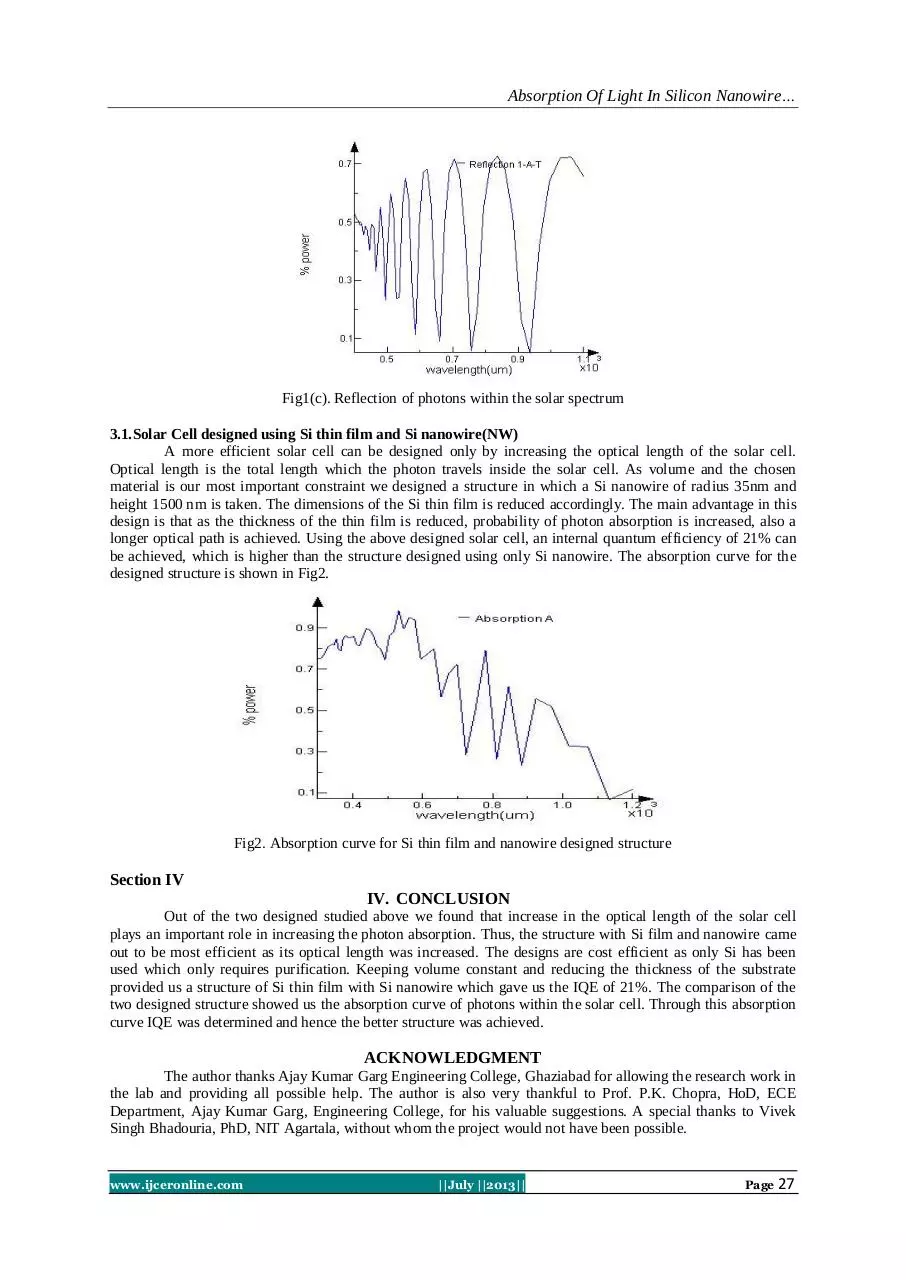
SOLAR CELL USING ONLY SI THIN FILM
In designing of the solar cell using only Si thin film, a cuboid of dimensions
(2500nm*2500nm*320nm) was taken. An illuminated source similar to that of solar spectrum within the range
400nm to 1100nm was applied over this thin film. As solar light consists of photons, these photons when fall
upon the film get absorbed, reflected and transmitted (5). The %power photons transmitted, absorbed and
reflected with respect to the wavelengths is shown in the figure 1(a), 1(b) and 1(c) respectively. For measuring
the above values various DFT monitors were used on several places in the designed solar cells, especially above
the film to measure the reflection, at the bottom of the film to measure the transmission and in between to
determine the absorbed photons. As photons are a source of energy, the graph is determined between %power
and wavelength. The overall energy is assumed to be 1. Thus once the transmission and absorption is
determined, reflection can be found using R=1-A-T (10,11).In designing this structure the main concern was
whether the structure is correctly designed or not, and whether the photon absorption will be maximum. For this
the absorption graph obtained was compared with the absorption curve obtained when Si was fabricated with
ZnO (3). On comparison it was found that the curve obtained was nearly similar within the spectrum range 0.6
to 0.9 µm.
Fig.1(a). Percent power transmitted wrt wavelength range 400nm to 1100nm
The variations in other wavelengths is due to the TCO used in the reference curve. This showed us that the
designed cell using Si thin film was nearly perfect to the fabricated design using ZnO. The internal quantum
efficiency which depends upon the photons absorbed came out to be 17%-19%.
Fig1(b). Absorption curve for photons entering the solar cell
www.ijceronline.com
||July ||2013||
Page 26
Absorption Of Light In Silicon Nanowire…
Fig1(c). Reflection of photons within the solar spectrum
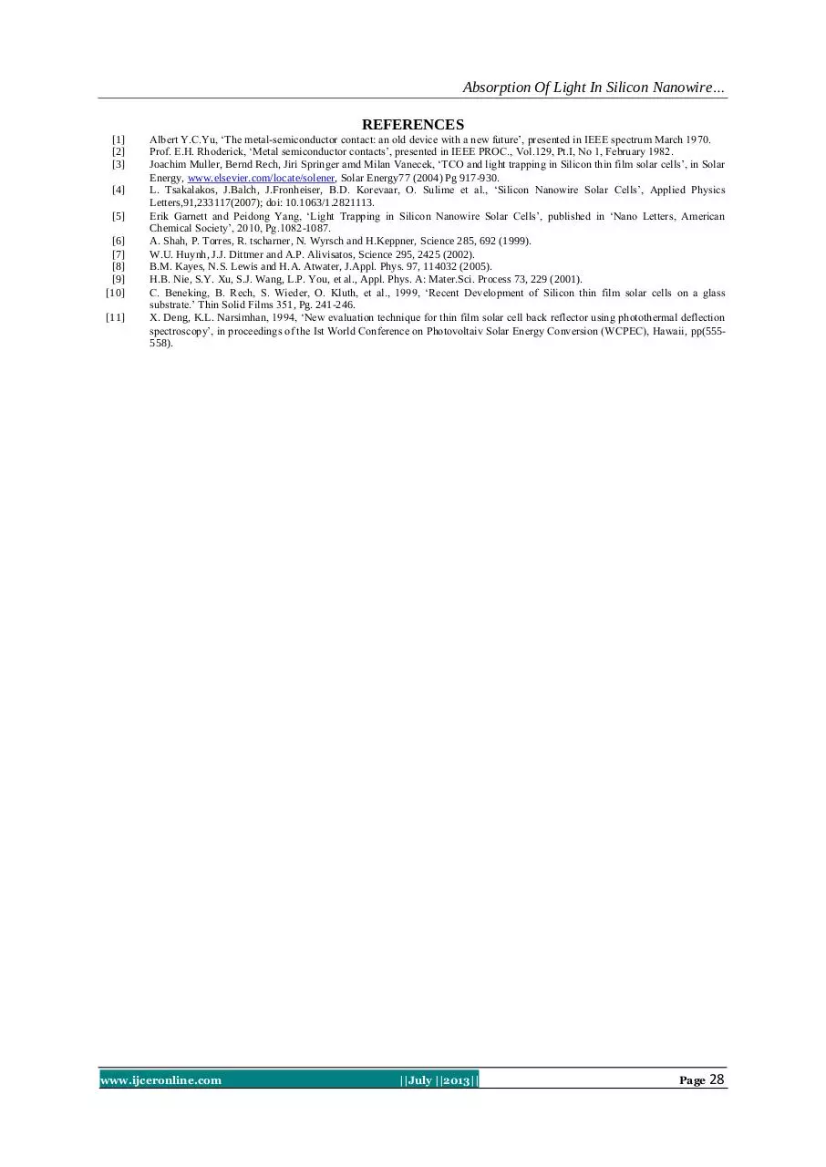
3.1.Solar Cell designed using Si thin film and Si nanowire(NW)
A more efficient solar cell can be designed only by increasing the optical length of the solar cell.
Optical length is the total length which the photon travels inside the solar cell. As volume and the chosen
material is our most important constraint we designed a structure in which a Si nanowire of radius 35nm and
height 1500 nm is taken. The dimensions of the Si thin film is reduced accordingly. The main advantage in this
design is that as the thickness of the thin film is reduced, probability of photon absorption is increased, also a
longer optical path is achieved. Using the above designed solar cell, an internal quantum efficiency of 21% can
be achieved, which is higher than the structure designed using only Si nanowire. The absorption curve for the
designed structure is shown in Fig2.
Fig2. Absorption curve for Si thin film and nanowire designed structure
Section IV
IV. CONCLUSION
Out of the two designed studied above we found that increase in the optical length of the solar cell
plays an important role in increasing the photon absorption. Thus, the structure with Si film and nanowire came
out to be most efficient as its optical length was increased. The designs are cost efficient as only Si has been
used which only requires purification. Keeping volume constant and reducing the thickness of the substrate
provided us a structure of Si thin film with Si nanowire which gave us the IQE of 21%. The comparison of the
two designed structure showed us the absorption curve of photons within the solar cell. Through this absorption
curve IQE was determined and hence the better structure was achieved.
ACKNOWLEDGMENT
The author thanks Ajay Kumar Garg Engineering College, Ghaziabad for allowing the research work in
the lab and providing all possible help. The author is also very thankful to Prof. P.K. Chopra, HoD, ECE
Department, Ajay Kumar Garg, Engineering College, for his valuable suggestions. A special thanks to Vivek
Singh Bhadouria, PhD, NIT Agartala, without whom the project would not have been possible.
www.ijceronline.com
||July ||2013||
Page 27
Absorption Of Light In Silicon Nanowire…
REFERENCES
[1]
[2]
[3]
[4]
[5]
[6]
[7]
[8]
[9]
[10]
[11]
Albert Y.C.Yu, ‘The metal-semiconductor contact: an old device with a new future’, presented in IEEE spectrum March 1970.
Prof. E.H. Rhoderick, ‘Metal semiconductor contacts’, presented in IEEE PROC., Vol.129, Pt.I, No 1, February 1982.
Joachim Muller, Bernd Rech, Jiri Springer amd Milan Vanecek, ‘TCO and light trapping in Silicon thin film solar cells’, in Solar
Energy, www.elsevier.com/locate/solener, Solar Energy77 (2004) Pg 917-930.
L. Tsakalakos, J.Balch, J.Fronheiser, B.D. Korevaar, O. Sulime et al., ‘Silicon Nanowire Solar Cells’, Applied Physics
Letters,91,233117(2007); doi: 10.1063/1.2821113.
Erik Garnett and Peidong Yang, ‘Light Trapping in Silicon Nanowire Solar Cells’, published in ‘Nano Letters, American
Chemical Society’, 2010, Pg.1082-1087.
A. Shah, P. Torres, R. tscharner, N. Wyrsch and H.Keppner, Science 285, 692 (1999).
W.U. Huynh, J.J. Dittmer and A.P. Alivisatos, Science 295, 2425 (2002).
B.M. Kayes, N.S. Lewis and H.A. Atwater, J.Appl. Phys. 97, 114032 (2005).
H.B. Nie, S.Y. Xu, S.J. Wang, L.P. You, et al., Appl. Phys. A: Mater.Sci. Process 73, 229 (2001).
C. Beneking, B. Rech, S. Wieder, O. Kluth, et al., 1999, ‘Recent Development of Silicon thin film solar cells on a glass
substrate.’ Thin Solid Films 351, Pg. 241-246.
X. Deng, K.L. Narsimhan, 1994, ‘New evaluation technique for thin film solar cell back reflector using photothermal deflection
spectroscopy’, in proceedings of the Ist World Conference on Photovoltaiv Solar Energy Conversion (WCPEC), Hawaii, pp(555558).
www.ijceronline.com
||July ||2013||
Page 28
Download E0371025028
E0371025028.pdf (PDF, 381.55 KB)
Download PDF
Share this file on social networks
Link to this page
Permanent link
Use the permanent link to the download page to share your document on Facebook, Twitter, LinkedIn, or directly with a contact by e-Mail, Messenger, Whatsapp, Line..
Short link
Use the short link to share your document on Twitter or by text message (SMS)
HTML Code
Copy the following HTML code to share your document on a Website or Blog
QR Code to this page

This file has been shared publicly by a user of PDF Archive.
Document ID: 0000134670.