HIOKI 1231 ENG (PDF)
File information
Title: BARE BOARD HiTESTER 1231
Author: HIOKI
This PDF 1.7 document has been generated by Adobe InDesign CS5.5_J (7.5.3) / Adobe PDF Library 9.9, and has been sent on pdf-archive.com on 24/12/2015 at 15:39, from IP address 5.18.x.x.
The current document download page has been viewed 472 times.
File size: 1.73 MB (4 pages).
Privacy: public file


File preview
BARE BOARD HiTESTER 1231
Automatic Testing Equipment
Faster, More Accurate, Easier
IC Package Board Tester
2
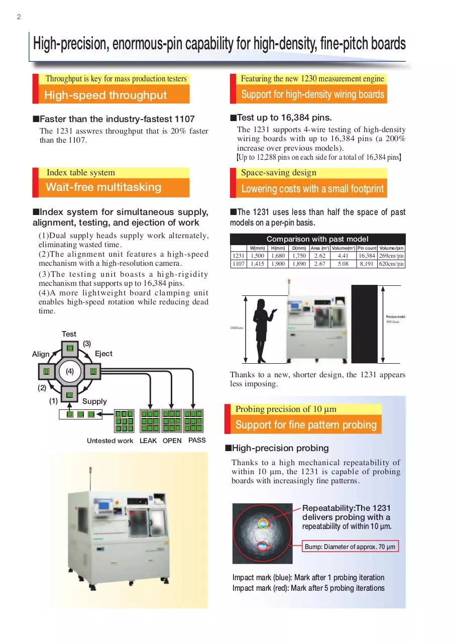
High-precision, enormous-pin capability for high-density, fine-pitch boards
Throughput is key for mass production testers
Featuring the new 1230 measurement engine
High-speed throughput
Support for high-density wiring boards
■Faster than the industry-fastest 1107
The 1231 asswres throughput that is 20% faster
than the 1107.
■Test up to 16,384 pins.
The 1231 supports 4-wire testing of high-density
wiring boards with up to 16,384 pins (a 200%
increase over previous models).
Up to 12,288 pins on each side for a total of 16,384 pins
Index table system
Space-saving design
Wait-free multitasking
Lowering costs with a small footprint
■Index system for simultaneous supply,
alignment, testing, and ejection of work
(1)Dual supply heads supply work alternately,
eliminating wasted time.
(2)The alignment unit features a high-speed
mechanism with a high-resolution camera.
(3)The testing unit boasts a high-rigidity
mechanism that supports up to 16,384 pins.
(4)A more lightweight board clamping unit
enables high-speed rotation while reducing dead
time.
■The 1231 uses less than half the space of past
models on a per-pin basis.
Comparison with past model
W(mm)
1231 1,500
1107 1,415
H(mm)
1,680
1,900
D(mm)
1,750
1,890
Area (m2) Volume(m3) Pin count Volume/pin
2.62
2.67
4.41
5.08
16,384 269cm /pin
8,191 620cm /pin
3
Previous model:
190.0cm
168.0cm
Test
3
(3)
Eject
Align
(4)
Thanks to a new, shorter design, the 1231 appears
less imposing.
(2)
(1)
Supply
Probing precision of 10 μm
Support for fine pattern probing
Untested work LEAK OPEN PASS
■High-precision probing
Thanks to a high mechanical repeatability of
within 10 μm, the 1231 is capable of probing
boards with increasingly fine patterns.
Repeatability:The 1231
delivers probing with a
repeatability of within 10 μm.
Bump: Diameter of approx. 70 μm
Impact mark (blue): Mark after 1 probing iteration
Impact mark (red): Mark after 5 probing iterations
3
Delivering measurement you can trust through easy operation
Detecting latent defects
One-touch fixtures
Respected HIOKI Measurement
Improved setup
■Open via measurement
Because wiring resistance and contact resistance
can be cancelled out with 4-terminal low-resistance
measurement, it is possible to detect minute
variations in resistance.
In order to detect pseudo-contact
and open vias, it is necessary to
use 4-terminal measurement with
an instrument that is both highresolution and high-precision.
■Test fixtures with a simple, one-touch mechanism
The 1231’s one-touch fixture design simplifies
setup changes by eliminating the need for previous
models’ time-consuming procedures for connecting
cables and acquiring test fixture offsets.
hOffsets only need to be acquired the first time a test fixture is used.
Slide
■Poor contact detection using 4-terminal measurement
Four-terminal measurement, a low-resistance measurement
method, is an effective way to detect open vias. However,
A 4-terminal
B
having
probes for all points would increase test
fixture cost.
The 1231 uses the independent 4-terminal method to limit
fixture cost while enabling reliable open via detection.
A
■There’s no need to change the board
clamping unit for boards that fall within the
size range of 13 × 13 mm to 55 × 55 mm.
■Four-terminal probe method
Four-terminal probes are
used for all points (2 probes
per point).
B
■Independent 4-terminal method
A
A
The independent 4-terminal
method can be used for
patterns like (A), halving the
number of probes required.
B
B
Support for lot process quality control
Pattern theoretical resistance test function
■Integration with U-ART TM
Enhanced measurement functionality enables
quality control of lot processes with a logical
resistance test function.
PASS region
FAIL
Within user-specified tolerance: PASS
Theoretical value: PASS
Manufacturing process is stable.
Within user-specified tolerance: PASS
FAIL
Manufacturing process is
subject to lot-specific process
variation or other factors.
Theoretical resistance value
(Act/Ref)
Manufacturing process is
subject to lot-specific process
variation or other factors.
Advanced yet easy-to-use functionality
Intuitive interface
■Newly designed software
Easy-to-understand icons help ensure intuitive
operation, and the 1231 can also graphically display
connection information for electronic components.
Mechanism
Measurement Unit
No. of test steps
Max. 10,000 steps
No. of test points
Max. 16,384 channels
(Upper: Max. 12,288 channels; lower: max. 4,096 channels)
Measurement ranges *
Resistors
Capacitors
Inductance
Diode VF measurement
Zener diode VZ measurement
Continuity testing
Insulation testing
X/Y-axis units
(upper and lower)
: 400mΩ to 2GΩ
: 10pF to 4mF
: 1μH to 100mF
: 0 to 25V
: 0 to 25V
: 0.4Ω to 400kΩ
: 4Ω to 40MW (DC)
: 50Ω to 200MΩ (HV)
θ-axis units
(upper and lower)
Z-axis units (upper and lower) Movement resolution: 1 μm
Transport height: 1,000 ±10 mm
Index table unit
Test fixtures
General Specifications
: 800mV to 250V f.s. (6 ranges)
: 100nA to 100mA f.s. (7 ranges)
: 10mA to 10mA rms (4 ranges)
Measurement unit *
DC voltmeter
DC ammeter
AC ammeter
Detection range
-99.9% to +999.9% or absolute value
Guarding *
5 points/step
AC 200 V ±10% (3-phase), 50/60 Hz
Power consumption: 6 kVA
Air pressure (primary): 0.6 to 0.99 MPa (dry air)
Set pressure (secondary): 0.5 ±0.1 MPa
Power supply
Air
Operating environment
* includes optional items
Accessories
options
1138-34
1138-35
1137-30
1139-56
1139-60
1937-30
1937-31
1937-32
1196
1134-02
1.5 sec(*Conditions: 2 points/pattern, 1,024 points, continuity
test, isolation test)
Min. supported board size: 13 × 13 mm
Max. supported board size: 75 × 75 mm
Max. no. of pins: Total of 16,384 (upper and lower)
Inter-probe pitch: Min. 80μm
Cycle time
HV voltage: 1V to 250V
Constant DC voltage : 100mV / 400mV (2 ranges)
Constant DC current : 200nA to 150mA (8 ranges)
Constant AC voltage : 0.1V rms (1 range)
Test signals *
Testable board size: 13 × 13 mm to 75 × 75 mm
(*Standard specifications: Up to 55 mm)
Measurable board thickness: 0.3 to 2.5 mm
(*Standard specifications: 0.8 to 2.5 mm)
Movement resolution: 1 μm
Rotation range: ±3° (during testing)
Operating temperature and humidity: 23°C ±3°C, 60% RH or less (non-condensing)
Storage temperature and humidity: 10°C to 43°C, 80% RH or less (non-condensing)
(Storage and operating conditions are the same for test heads.)
Atmosphere: Avoid use in the presence of dust, mechanical
vibration, corrosive gas, etc.
Floor strength: At least 700 kg/m2
Computer accessories (keyboard, etc.), thermal printer, printer cable
Factory options
General-purpose scanner board: Semiconductor switches (128 channels per board, with guarding)
Upper alignment camera (Z-axis)
1107 test head support
General-purpose scanner board: Semiconductor switches (128 channels per board, without guarding)
Data composition software
FL-Link7 FLY-LINE (data linking software)
EPA-Link (data linking software for boards with embedded passive and active devices)
AC measurement function (low-capacitance measurement)
DC measurement function (low-resistance measurement)
MLCC measurement
Printer paper (1 box of 10 rolls)
Probe impact sheet
1231 External Dimensions
(reference diagram)
Model
1231
HiTESTER dimensions
Approx. 1,500 (W) × 1,680 (H) × 1,750 (D) mm1
Weight
Approx. 2,000 kg
1Varies with specifications.
For more information, contact your nearest Sales Office.
Note: Company names and Product names appearing in this catalog are trademarks or registered trademarks of various companies.
HIOKI (Shanghai) SALES & TRADING CO., LTD.:
TEL +86-21-63910090 FAX +86-21-63910360
http://www.hioki.cn / E-mail: info@hioki.com.cn
РАДАР - ОФИЦИАЛЬНЫЙ ДИЛЕР HIOKI
HIOKI INDIA PRIVATE LIMITED:
TEL +91-124-6590210 FAX +91-124-6460113
HEADQUARTERS:
E-mail: hioki@hioki.in
81 Koizumi, Ueda, Nagano, 386-1192, Japan
TEL +81-268-28-0562 FAX +81-268-28-0568 HIOKI SINGAPORE PTE. LTD.:
http://www.hioki.com / E-mail: os-com@hioki.co.jp TEL +65-6634-7677 FAX +65-6634-7477
E-mail: info-sg@hioki.com.sg
HIOKI USA CORPORATION:
HIOKI KOREA CO., LTD.:
TEL +1-609-409-9109 FAX +1-609-409-9108 TEL +82-42-936-1281 FAX +82-42-936-1284
http://www.hiokiusa.com / E-mail: hioki@hiokiusa.com E-mail: info-kr@hioki.co.jp
All information correct as of May. 15, 2013. All specifications are subject to change without notice.
РОССИЯ, 198152, Санкт-Петербург
Краснопутиловская ул., д.25
Тел./факс +7 (812) 600-48-89
Тел.: +7 (812) 375-32-44
www.radar1.ru
1231E6-35M
Printed in Japan
info@radar1.ru
Download HIOKI 1231 ENG
HIOKI_1231_ENG.pdf (PDF, 1.73 MB)
Download PDF
Share this file on social networks
Link to this page
Permanent link
Use the permanent link to the download page to share your document on Facebook, Twitter, LinkedIn, or directly with a contact by e-Mail, Messenger, Whatsapp, Line..
Short link
Use the short link to share your document on Twitter or by text message (SMS)
HTML Code
Copy the following HTML code to share your document on a Website or Blog
QR Code to this page

This file has been shared publicly by a user of PDF Archive.
Document ID: 0000326461.