Final (PDF)
File information
This PDF 1.5 document has been generated by TeX / pdfTeX-1.40.16, and has been sent on pdf-archive.com on 16/12/2016 at 18:43, from IP address 174.53.x.x.
The current document download page has been viewed 429 times.
File size: 5.57 MB (11 pages).
Privacy: public file


File preview
An Investigation into Nanoparticle Fabrication
Mitchell Fontaine
December 9, 2016
Abstract
In this paper, methods of fabricating gold nanoparticles are investigated with respect to
their feasibility within the context of the Bethel University Nanotechnology Lab. Of the
two methods investigated, electrodeposition by field-induced atomic emission was not
accomplished, but thermal deposition onto exposed PMMA resist proved to have high
potential for successful nanoparticle fabrication.
Introduction
Nanoparticles are of importance in many
fields, such as material science, electrical
engineering, optics, and, of course, nanotechnology. Particularly, gold nanoparticles have applications in optical/plasmonic
tweezing, solar cell doping, cancer treatment, infrared detectors, and many other
uses. However, a challenge facing many
scientists and engineers is developing a
method to fabricate such particles. One
such method, which is explored in this paper, is electrodeposition by electric fieldinduced atomic emission. Essentially this
method involves applying a voltage across
a gold wire and silicon chip, separated
by a sub-nm gap. This creates an electric field, and some gold atoms migrate
from the tip of the wire to the silicon chip.
Now, in order to accomplish this, one must
have a means to control the tip of the
wire in three dimensions, as well as keep
it very close to the surface of the chip. A
tool that works well for this purpose is an
Atomic Force Microscope (AFM). Knowledge of the basic principles of the mechanisms and operation of the AFM are necessary if one is to follow this procedure.
Atomic Force Microscopy (AFM)
Operation of an AFM relies on the dipoledipole interaction between atoms. An
AFM utilizes these forces to map out a
topographic image of a surface. A small
quartz tuning fork, shown in Figure 1, is
attached to the AFM, and when a voltage is applied to the tuning fork, it resonates at its specific resonance frequency.
A very sharp tungsten tip, ideally with
an apex diameter on the order of tens of
nm or less, is attached to the end of the
tuning fork. A photograph of one such is
shown in Figure 1. When the sharp end
of this tip comes very close to the surface
being imaged (gap one nm or less), the
dipole-dipole interaction from the atoms
in the tip and the atoms in the surface
damp the resonance of the tuning fork.
The AFM system moves the tip up or
down to to hold the damping constant as
the tip is moved across the surface, and a
topographic image of the surface can be
1
Figure 1: Tuning fork probe
generated. To use an AFM for electrodeposition, the tungsten tip is replaced with
a gold wire, which is then connected to
the negative terminal of a function generator. A silicon chip is used as the deposition surface, with a small piece of indium melted onto a corner as an electrical
contact, which is in turn connected to the
positive terminal of the aforementioned
function generator. For the purposes of
this lab, a GWInstek AFT-2125 was used.
However, there are many hurdles to overcome in making this process work effec-
tively, as the author of this paper discovered. For the AFM to function properly,
the tuning fork must be electrically isolated. This proved to be somewhat difficult, as the gold wire (which has a voltage
applied to it) is glued to the tuning fork,
causing the electrical pulses applied to the
tip to interfere with the AFM resonance
feedback loop. However, it seemed that
this interference could be overcome, and
the experiment was able to continue. An
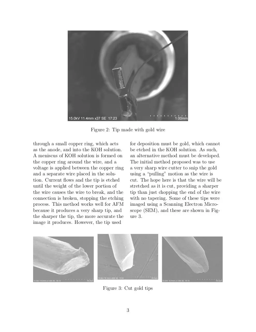
image of one of these tips with a gold wire
glued to a tuning fork is shown if Figure 2.
Tip Preparation
An important aspect of this process is
the sharpness of the tip used for imaging/deposition. The tungsten tips for con-
ventional imaging were prepared using
electrochemical etching in a KOH solution.
The wire to be used for the tip is placed
2
Figure 2: Tip made with gold wire
through a small copper ring, which acts
as the anode, and into the KOH solution.
A meniscus of KOH solution is formed on
the copper ring around the wire, and a
voltage is applied between the copper ring
and a separate wire placed in the solution. Current flows and the tip is etched
until the weight of the lower portion of
the wire causes the wire to break, and the
connection is broken, stopping the etching
process. This method works well for AFM
because it produces a very sharp tip, and
the sharper the tip, the more accurate the
image it produces. However, the tip used
for deposition must be gold, which cannot
be etched in the KOH solution. As such,
an alternative method must be developed.
The initial method proposed was to use
a very sharp wire cutter to snip the gold
using a “pulling” motion as the wire is
cut. The hope here is that the wire will be
stretched as it is cut, providing a sharper
tip than just chopping the end of the wire
with no tapering. Some of these tips were
imaged using a Scanning Electron Microscope (SEM), and these are shown in Figure 3.
Figure 3: Cut gold tips
3
Imaging
Figure 4: AFM scans with gold tip
4
Once tips were constructed, the next
step was determining their effectiveness/accuracy in imaging a surface. Several scans were taken using these tips,
some of which are shown in Figure . The
primary goal of these scans was to determine if the gold tips would accurately image the topography of the surface (i.e. flat,
curved, rough, etc), if the images were reproducible (if two scans of the same surface generated the same image), and the
resolution of the images (minimum size
of surface features that can be imaged).
In taking these scans, it was found that
these tips often exhibited unpredictable
behavior. There were many instances were
an image would not accurately depict the
surface, or two scans of the same surface
would appear different. However, once the
system was recalibrated a few times, the
tips seemed to function better, and more
accurate images were taken. It was found
that the images were accurate to about 1
µm, indicating that the tips had an apex
diameter on the order of a few µm.
Deposition
Figure 6: After attempted deposition
Figure 5: Before attempted deposition
In developing a method for electrodeposition, the voltage applied to the tip
must be pulsed (rather than continuous,
i.e. DC), as this is meant to create small
nanoparticles with each pulse, rather than
a continuous deposition. The pulses should
alternate between zero and a positive voltage, so signal from the function genera5
Figure 7: Etched gold tip
from there. Since the recommended pulse
duration covered such a wide range, an
initial pulse of 1 ms was chosen, corresponding to an output frequency of 1
kHz from the function generator. Images of the before and after scans from
this trial are shown in Figures 5 and 6.
These scans show essentially the same
surface topography, indicating a lack of
deposited gold nanoparticles. In subsequent tests, the voltage was increased to
2, 5, 7.5, 10, and 13.6 (the maximum output amplitude of the function generator)
V , and pulse lengths were varied to 2, 4,
10, 50, and 100 ms. Despite these variations, no gold deposition was observed. It
was suggested that perhaps scans were being taken too quickly, and the probe tip
was not picking up the small surface imperfections indicating gold deposition. To
test this hypothesis, several scans were
taken at slower speeds. This slowed-down
process was accomplished by extending
the read/write delay in the scanning feedback loop. The standard delay is 10 ms, so
scans were taken with delays of 20, 40, and
tor must have a DC offset to always stay
above zero. The primary variable then, is
the strength and duration of the pulses.
In [1], it was recommended to use a tipnegative voltage of 20 V , with pulses from
0.2 - 200 milliseconds. Clearly, this is a
rather broad range, so some experimentation was needed. The end of the gold wire
used for the tip was connected to the negative terminal of the function generator,
and an alligator clip connected to the positive terminal was clamped on the indium
contact of the silicon wafer. The method
for testing deposition is as follows: first,
with no voltage applied, a scan is taken
of a square area with edges 5-10 µm in
length. Then, another scan is performed,
this time with the voltage pulse applied,
over a 1 µm2 area in the middle of the initial area. Once that is finished, the voltage
is turned off, and another scan is taken of
the first, larger area. By comparing the
first and last scans, the hope is that the
deposited nanoparticles can be observed.
At first, 20 V seemed rather high, so the
initial bias was 1 V , and was increased
6
even up to 100 ms, but these scans still
did not indicate the presence of nanoparticles. After some frustration and review
of the literature, it was noted that many
other papers used tips much sharper than
the 1 µm tip used here. The decision was
made to try electrochemically etching gold
tips, similar to the Tungsten tips etched
previously. In reference [3], gold tips were
etched using a solution 0.5 M in HCl and
0.5 M in H2 SO4 . This solution was prepared, and etching was accomplished using
an applied voltage of 24 V DC in about
10 minutes. Etching appeared successful,
so deposition was tried using this tip, but
nanoparticles were not observed. Seeking
insight into why deposition was again a
failure, the etched tip was imaged in the
SEM, and this image is seen in Figure 7.
As can be seen, the tip does not have the
nanometer sharpness that is desirable, but
instead exhibits a curl at the end. This
is most likely due to the softness of gold
compared to Tungsten. In the etching process, instead of making a clean break at
the tip as Tungsten does, the gold may
have stretched and broke instead, causing the tip to recoil and form the curl
shape seen in the figure. This tip geometry explains why it failed to deposit any
nanoparticles.
PMMA Resist Exposure
At this point, upon further review of the
literature, it was noted that nanoparticles fabricated in Reference [2] were only
a few hundred Angstroms in height and
diameter. While the AFM is capable of
taking images at this vertical resolution,
there is often noise on this scale, so it is
possible the AFM may not have imaged
the nanoparticles. However, it is much
more likely that the poor tip geometry
was interfering with successful deposition.
As such, the research advisor proposed
an alternative method to fabricate gold
nanoparticles by etching PMMA and then
using a thermal deposition chamber. The
method for such a procedure is outlined as
follows.
PMMA, or Poly(methyl methacrylate), is
spin-coated onto a silicon chip, which produces a coating on the chip a few hundred
nm thick (here, 950 K molecular weight
PMMA is used). Reference [4] advised using a PMMA coating around 20 nm thick,
so the coating used in this process is not
ideal, but due to time constraints of this
project, it was used anyway. The coated
chip is then placed on the imaging stage
of the AFM and connected to the positive terminal of a DC power supply. The
negative terminal connected to the AFM
wire tip. When the DC voltage is applied
between the AFM tip and the PMMAcoated silicon chip, electrons tunnel from
the AFM tip to the silicon, leaving behind
an area of broken-up polymers where the
PMMA was. The chip is then placed in
a developer solution of 1 part MBIK to 3
parts isopropyl alcohol. The developer removes the broken-up polymers, exposing a
small area of silicon which acts as a mold
for gold to be deposited into. While Reference [4] used a tip-negative bias of 40
V DC, the method performed here used
63 V . This was done because the PMMA
coating was much thicker than that used
in [4], and 63 V is the maximum output
of the DC power supply. When using the
AFM tip to expose an area of PMMA, it
7
Figure 8: Microscopic image of removed PMMA
was decided to expose three square areas
of 25 µm2 each, arranged geometrically, in
order to make the results more easily observable. After the chip was placed in the
developer solution for about 30 seconds,
it was examined initially under an optical microscope. This examination did not
indicate successful removal of the PMMA
substrate. The procedure was was tried a
few more times, but to no avail. At this
point, the researcher decided that perhaps
something just wasn’t working quite correctly in the AFM set up, and decided
to try exposing the PMMA manually. To
yield clearer results, a 0.25 mm diameter wire was used, rather than the 0.05
mm gold wire used previously. The wire
was placed in a precision manipulator and
connected to the negative terminal of the
DC power supply and 63 V was applied.
As before, the positive terminal was connected to the PMMA-coated silicon chip.
The wire was contacted to the chip and
maintained contact for about 15 seconds.
The power supply indicated a current 0.01
A was flowing at this time. Contact was
then broken, and the wire was touched to
the chip in a few other places for about
the same amount of time. The chip was
then placed in the developer solution for
about a minute and examined under an
optical microscope.
This indicated large areas of exposed silicon where the wire contacted the chip.
An image of one of these areas is shown in
Figure 8. The elongated shape of this area
indicates that the wire actually scraped
across the surface as it made contact,
8
Figure 9: Areas showing chromium deposition
rather than just at single point. In any
case, the PMMA was removed in this area,
so the procedure was continued, and deposition was attempted. While the initial plan was to fabricate gold nanoparticles, at the time of the experiment the
thermal deposition chamber was only
set up to deposit chromium. Due to the
time constraints of the project, chromium
was used, the idea being that, if the process worked with chromium, it would
work with gold. The deposition chamber was often extremely uncooperative
during this process, but eventually 50
nm of chromium was deposited onto the
chip. The chip was then placed in an acetone bath. This breaks down and removes
PMMA coating, leaving behind only the
chromium that was deposited directly onto
the silicon, and not the PMMA. After resting in the acetone for a few minutes, the
chip was examined under an optical microscope. This was rather unclear, as the
etched areas appeared essentially the same
as before deposition. The chip was then
imaged in an SEM, as the SEM is more
effective in conveying the depth of an image (i.e. the area where chromium was
retained on the chip should appear higher
than the naked silicon surface). An image from the SEM is shown in Figure 9,
where it appears that the area where the
PMMA was etched retained the chromium
coating. The indicates that this method
has strong potential, with some tweaking,
for successfully fabricating gold nanoparticles. However, these chromium areas were
about 0.1 mm in width, 1 mm in length,
and about 50 nm in thickness. This size
and shape is not idea, but, again, the important thing is that this represents that
the process does work. In an attempt to
move closer to the desired nanoparticle
size and shape, this manual etching process was repeated on a new chip, this time
using the 0.05 mm diameter gold wire, in
order to expose smaller areas. After using the same method as the larger wire,
the chip was examined under the optical
microscope. While this examination was
not incredibly conclusive, there were small
areas that appeared to be exposed when
9
Download Final
Final.pdf (PDF, 5.57 MB)
Download PDF
Share this file on social networks
Link to this page
Permanent link
Use the permanent link to the download page to share your document on Facebook, Twitter, LinkedIn, or directly with a contact by e-Mail, Messenger, Whatsapp, Line..
Short link
Use the short link to share your document on Twitter or by text message (SMS)
HTML Code
Copy the following HTML code to share your document on a Website or Blog
QR Code to this page

This file has been shared publicly by a user of PDF Archive.
Document ID: 0000523245.