RDA1846 RDA (PDF)
File information
Title: ÿþh�t�t�p�:�/�/�w�w�w�.�D�a�t�a�S�h�e�e�t�4�U�.�c�o�m���
Author: ÿþh�t�t�p�:�/�/�w�w�w�.�D�a�t�a�S�h�e�e�t�4�U�.�c�o�m���
This PDF 1.5 document has been generated by Acrobat PDFMaker 9.0 Word 版 / ÿþS�c�a�n�S�o�f�t� �P�D�F� �C�r�e�a�t�e�!���, and has been sent on pdf-archive.com on 22/10/2017 at 19:12, from IP address 80.147.x.x.
The current document download page has been viewed 554 times.
File size: 624.56 KB (16 pages).
Privacy: public file

File preview
RDA1846
SINGLE CHIP TRANSCEIVER FOR WALKIE TALKIE
Rev.1.2–Dec.2009
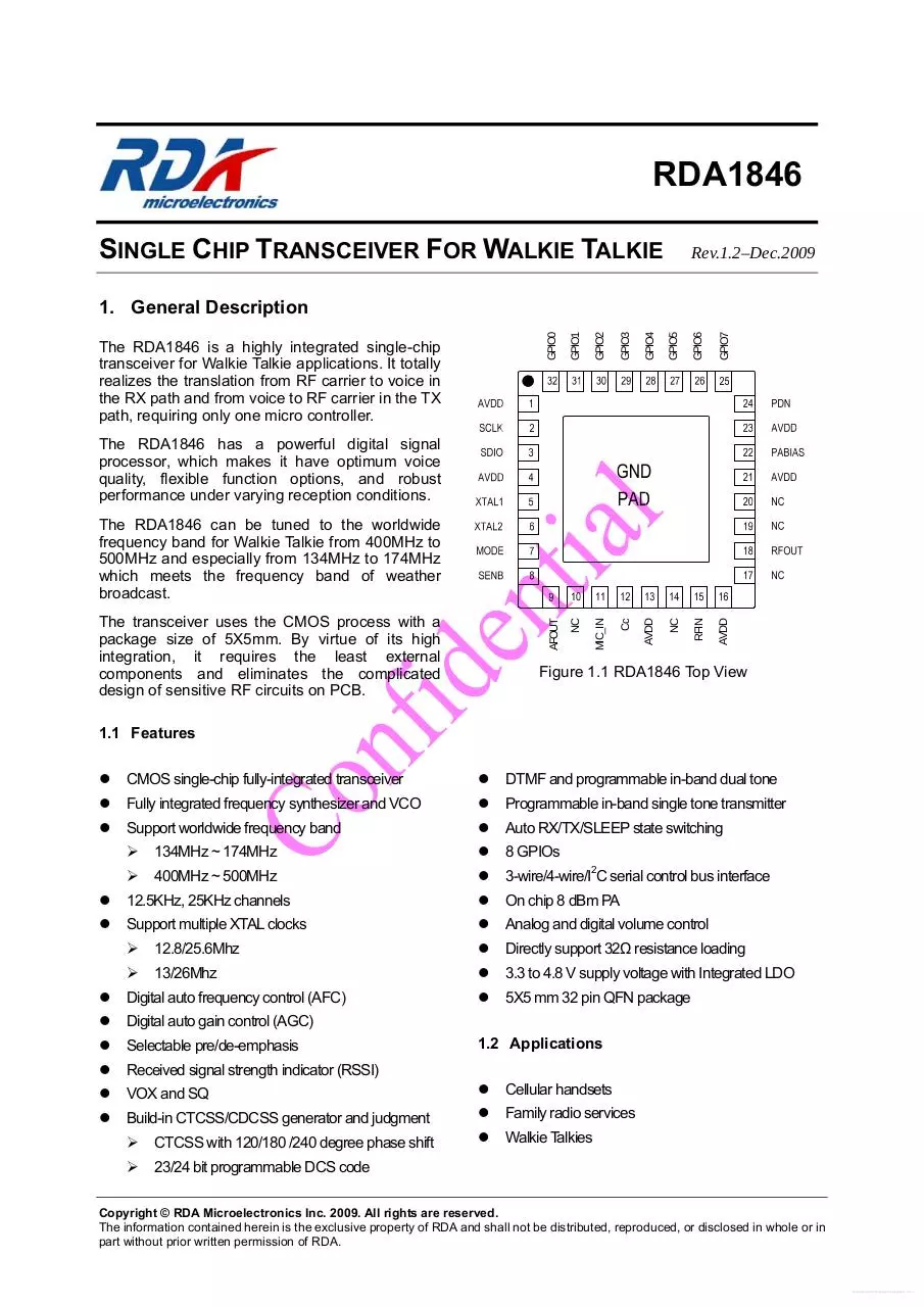
GPIO0
GPIO1
GPIO2
GPIO3
GPIO4
GPIO5
GPIO6
GPIO7
NC
MIC_IN
Cc
AVDD
NC
RFIN
AVDD
The RDA1846 is a highly integrated single-chip
transceiver for Walkie Talkie applications. It totally
realizes the translation from RF carrier to voice in
the RX path and from voice to RF carrier in the TX
path, requiring only one micro controller.
AFOUT
1. General Description
The RDA1846 has a powerful digital signal
processor, which makes it have optimum voice
quality, flexible function options, and robust
performance under varying reception conditions.
The RDA1846 can be tuned to the worldwide
frequency band for Walkie Talkie from 400MHz to
500MHz and especially from 134MHz to 174MHz
which meets the frequency band of weather
broadcast.
The transceiver uses the CMOS process with a
package size of 5X5mm. By virtue of its high
integration, it requires the least external
components and eliminates the complicated
design of sensitive RF circuits on PCB.
Figure 1.1 RDA1846 Top View
1.1 Features
CMOS single-chip fully-integrated transceiver
DTMF and programmable in-band dual tone
Fully integrated frequency synthesizer and VCO
Programmable in-band single tone transmitter
Support worldwide frequency band
Auto RX/TX/SLEEP state switching
134MHz ~ 174MHz
8 GPIOs
400MHz ~ 500MHz
3-wire/4-wire/I2C serial control bus interface
12.5KHz, 25KHz channels
On chip 8 dBm PA
Support multiple XTAL clocks
Analog and digital volume control
12.8/25.6Mhz
Directly support 32Ω resistance loading
13/26Mhz
3.3 to 4.8 V supply voltage with Integrated LDO
5X5 mm 32 pin QFN package
Digital auto frequency control (AFC)
Digital auto gain control (AGC)
Selectable pre/de-emphasis
Received signal strength indicator (RSSI)
VOX and SQ
Cellular handsets
Build-in CTCSS/CDCSS generator and judgment
Family radio services
CTCSS with 120/180 /240 degree phase shift
Walkie Talkies
23/24 bit programmable DCS code
1.2 Applications
Copyright © RDA Microelectronics Inc. 2009. All rights are reserved.
The information contained herein is the exclusive property of RDA and shall not be distributed, reproduced, or disclosed in whole or in
part without prior written permission of RDA.
Free Datasheet http://www.Datasheet4U.com
2. Table of Contents
1.
General Description ....................................................................................................................................1
1.1
Features........................................................................................................................................1
1.2
Applications .................................................................................................................................1
2. Table of Contents.........................................................................................................................................2
3. Functional Description................................................................................................................................3
3.1
RF input and output .......................................................................................................................3
3.2
Voice input and output................................................................................................................4
3.3
Synthesizer ...................................................................................................................................4
3.4
XTAL Clock .................................................................................................................................4
3.5
DSP functions...............................................................................................................................4
3.6
Integrated LDO ...........................................................................................................................4
3.7
Serial Control Interface ..............................................................................................................4
4. Electrical Characteristics ...........................................................................................................................5
5. Receiver/Transmitter Characteristics .......................................................................................................6
6. Control Interface Characteristics ..............................................................................................................7
7. Pins Description...........................................................................................................................................8
8. Application Diagram................................................................................................................................. 11
9. Package Outline.........................................................................................................................................12
10. Solder Mounting Condition......................................................................................................................13
11. Change List................................................................................................................................................16
12. Contact Information .................................................................................................................................16
Copyright © RDA Microelectronics Inc. 2009. All rights are reserved.
The information contained herein is the exclusive property of RDA and shall not be distributed, reproduced, or disclosed in whole or in
part without prior written permission of RDA.
Free Datasheet http://www.Datasheet4U.com
RDA Microelectronics, Inc.
RDA1846 SPEC V1.2e
Switch
Antana
3. Functional Description
…
Figure 3.1 RDA1846 Block Diagram
The RDA1846 transceiver features very low solution cost and reduced complexity. As shown in Fig.3.1, to
totally complete the translation from RF carrier to voice in the RX path and from voice to RF carrier in the
TX path, the chip integrates nearly all the functional blocks including RF and base band analog blocks
and digital signal processor. It requires only one micro controller and a few external components to
realize a walkie-talkie.
A powerful integrated DSP accomplishes both the demodulation and modulation of the FM signal.
Besides, standard walkie-talkie features such as CTS, CDS, VOX and SQ etc. are provided through the 8
GPIOs of the chip. Especially, by virtue of the state-of-the-art CMOS technology advanced algorithms
such as AFC, AGC, RSSI and SNR calculations are realized in the DSP, which guarantees the high
receiving and transmitting quality while still consumes a low power. Flexible RX/TX/SLEEP auto switching
function from the DSP further reduces the average power consumptions.
LDOs are also integrated in the chip which further reduces the BOMs.
All interface pins of the chip will be shortly explained below. For details, refer to the ‘RDA 1846
programming guide’.
3.1 RF input and output
The chip can receive and transmit RF signals from 400 to 500MHz and from 134 to 174MHz which cover
most of the walkie-talkie frequency bands around the world and the weather broadcast band. For the RF
input, a direct-in connection from the antenna to the LNA input pin through a switch is suggested which
means no input impedance matching is needed for the receive band. For the RF out, a pa diver can
deliver no more than 8 dBm power to PA. PA bias voltage from 1.5V~2.8V for the power amplifier can be
supplied from the PABIAS pin.
The information contained herein is the exclusive property of RDA and shall not be distributed, reproduced, or disclosed in whole or in
part without prior written permission of RDA.
Page 3 of 16
Free Datasheet http://www.Datasheet4U.com
RDA Microelectronics, Inc.
RDA1846 SPEC V1.2e
3.2 Voice input and output
In the RX path, the voice signal after demodulation is sent to the internal DAC which can directly drive a
32Ω resistance loading through AC coupling. In the TX path, microphone signal can be sent into the chip through AC
coupling capacitors.
3.3 Synthesizer
The frequency synthesizer generates the local oscillator signal. All building blocks are fully integrated
without any external components. LO frequency can be programmed through the serial interface by the
MCU. (How to select frequency band and program LO frequency, refer to the programming guide)
3.4 XTAL Clock
The RDA1846 supports XTAL clocks such as 12.8 MHz, 13 MHz, 25.6 MHz and 26 MHz. The internal XTAL
oscillator can also be bypassed thus TCXO clock with appropriate amplitude can be sent into the chip directly. (How
to configure the internal XTAL oscillator, refer to the programming guide)
3.5 DSP functions
The DSP accomplishes the demodulation and modulation of the FM signal. Standard walkie-talkie
features such as CTS, CDS, VOX and SQ etc. are provided through the 8 GPIOs. (How to configure the
GPIOs, refer to the programming guide)
3.6 Integrated LDO
LDOs are integrated on chip which eliminates using one LDO chip on the PCB. Supply voltage for the chip is
suggested to be within 3.3V~4.8V. A common share of the supply voltage for RDA1846 and other chips or on board
circuits are not appropriate and thus not recommended.
3.7 Serial Control Interface
A 3-wire/4-wire/I2C serial interface is provided for host IC to read and write RDA1846 control registers.
(For details of the serial control interface, refer to the programming guide).
The information contained herein is the exclusive property of RDA and shall not be distributed, reproduced, or disclosed in whole or in
part without prior written permission of RDA.
Page 4 of 16
Free Datasheet http://www.Datasheet4U.com
RDA Microelectronics, Inc.
RDA1846 SPEC V1.2e
4. Electrical Characteristics
Table 4-1
DC Electrical Specification (Recommended Operation Conditions):
SYMBOL
DESCRIPTION
MIN
TYP
MAX
UNIT
AVDD
Supply Voltage from battery or LDO
3.3
3.3
4.8
V
Tamb
Ambient Temperature
-25
27
+85
℃
VL
CMOS Low Level Input/output Voltage
0
0.3
V
VH
CMOS High Level Input/output Voltage
2.7
3
V
VTH
CMOS Threshold Voltage
Table 4-2
1.5
V
DC Electrical Specification (Absolute Maximum Ratings):
SYMBOL
DESCRIPTION
MIN
TYP
MAX
UNIT
Tamb
Ambient Temperature
-40
+90
°C
IIN
Input Current
-10
+10
mA
VIN
Input Voltage
-0.3
3.3
V
Vlna
LNA Input Level
+10
dBm
Table 4-3
Power consumption specification
(AVDD = 3.3 V, TA = -25 to 85℃, unless otherwise specified)
STATE
DESCRIPTION
Condition
TYP
UNIT
IRx
Continue Receive
RXON=1,PDN=1
55
mA
ITx
Continue Transmit
TXON=1,PDN=1
50
mA
Isleep
Deep sleep
PDN=0
40
A
The information contained herein is the exclusive property of RDA and shall not be distributed, reproduced, or disclosed in whole or in
Page 5 of 16
part without prior written permission of RDA.
Free Datasheet http://www.Datasheet4U.com
RDA Microelectronics, Inc.
5.
RDA1846 SPEC V1.2e
Receiver/Transmitter Characteristics
Table 5-1
Receiver Characteristics
(AVDD = 3.3 V, TA = -25 to 85 °C, unless otherwise specified)
SYMBOL
PARAMETER
CONDITIONS
MIN
TYP
MAX
UNIT
General specifications
Fin
Input Frequency Range1
400
520
MHz
Input Frequency Range2
134
174
MHz
Input Frequency Range3
200
260
MHz
NF
Noise Figure
IP3in
Input IP3
SEN
Sensitivity
ACS
IR
Adjacent Channel Selectivity
Max RX Gain
Max RX Gain
12.5kHz channel,
12dB SINAD
±12.5KHz
Image rejection
Blocker
3
-10
-6
0
dBm
-125
-124
-123
dBm
65
66
67
dB
60
70
dB
85
dB
1.5
%
> 1MHz
Voice distortion
Table 5-2
dB
Transmit Characteristics
(AVDD = 3.3 V, TA = -25 to 85°C, unless otherwise specified)
SYMBOL
PARAMETER
CONDITIONS
MIN
TYP
MAX
UNIT
General specifications
Fout
POUT
Output Frequency Range1
400
520
MHz
Output Frequency Range2
134
174
MHz
Output Frequency Range3
200
260
MHz
8
dBm
Output Power
-2
SINAD/SNR
ACP
5
48/53
dB
-67
dBc
13
mV
Voice distortion
0.5
%
Modulation limitation
2.2
Adjacent channel power
Modulation sensitivity
1.5kHz frequency offset
2.5
kHz
The information contained herein is the exclusive property of RDA and shall not be distributed, reproduced, or disclosed in whole or in
Page 6 of 16
part without prior written permission of RDA.
Free Datasheet http://www.Datasheet4U.com
RDA Microelectronics, Inc.
RDA1846 SPEC V1.2e
6. Control Interface Characteristics
Refer to the ‘RDA1846 programming guide’.
The information contained herein is the exclusive property of RDA and shall not be distributed, reproduced, or disclosed in whole or in
Page 7 of 16
part without prior written permission of RDA.
Free Datasheet http://www.Datasheet4U.com
RDA Microelectronics, Inc.
RDA1846 SPEC V1.2e
7. Pins Description
Figure 7.1 RDA1846 Top View
The information contained herein is the exclusive property of RDA and shall not be distributed, reproduced, or disclosed in whole or in
Page 8 of 16
part without prior written permission of RDA.
Free Datasheet http://www.Datasheet4U.com
RDA Microelectronics, Inc.
Table 7-1
RDA1846 SPEC V1.2e
RDA1846 Pins Description
SYMBOL
PIN
DESCRIPTION
AVDD
1
Power supply
SCLK
2
Clock input for serial control bus
SDIO
3
Data input/output for serial control bus
AVDD
4
Power supply
XTAL1
5
Oscillator pin 1
XTAL2
6
Oscillator pin 2
Control Interface select
MODE
7
When MODE = VL, I2C Interface is select
When MODE = VH, SPI Interface is select
SENB
8
Latch enable (active low) input for serial control bus
AFOUT
9
Audio signal output to speaker
NC*
10
No connection
MIC_IN
11
MIC input
Cc
12
Compensation capacitor connection pin
AVDD
13
Power supply
NC*
14
No connection
RFIN
15
RF signal input
AVDD
16
Power supply
NC*
17
No connection
RFOUT
18
RF signal output
NC*
19
No connection
NC*
20
No connection
AVDD
21
Power supply
PABIAS
22
PA bias supply for PA
AVDD
23
Power supply
PDN
24
Chip enable, low active
GPIO7
25
GPIO6
26
GPIO5
27
GPIO4
28
GPIO3
29
Gpio7 / vox
(When Gpio7=VH, vox is active; else VL)
Gpio6 / sq
(When Gpio6=VH, sq is active; else VL)
Gpio5 / txon
(When Gpio5=VH, txon is active; else VL)
Gpio4 / rxon
(When Gpio4=VH, rxon is active; else VL)
Gpio3 / sdo
(Gpio3=VH or VL, it is the output register data in 4 wire control
interface mode)
GPIO2
30
Gpio2 / int
(When Gpio2=VH, int is active; else VL)
The information contained herein is the exclusive property of RDA and shall not be distributed, reproduced, or disclosed in whole or in
Page 9 of 16
part without prior written permission of RDA.
Free Datasheet http://www.Datasheet4U.com
Download RDA1846-RDA
RDA1846-RDA.pdf (PDF, 624.56 KB)
Download PDF
Share this file on social networks
Link to this page
Permanent link
Use the permanent link to the download page to share your document on Facebook, Twitter, LinkedIn, or directly with a contact by e-Mail, Messenger, Whatsapp, Line..
Short link
Use the short link to share your document on Twitter or by text message (SMS)
HTML Code
Copy the following HTML code to share your document on a Website or Blog
QR Code to this page

This file has been shared publicly by a user of PDF Archive.
Document ID: 0000687777.