Cheat Sheet 3 (PDF)
File information
This PDF 1.4 document has been generated by Adobe InDesign CS6 (Windows) / Adobe PDF Library 10.0.1, and has been sent on pdf-archive.com on 20/10/2015 at 05:35, from IP address 73.1.x.x.
The current document download page has been viewed 946 times.
File size: 344.16 KB (2 pages).
Privacy: public file

File preview
AND-OR
THE NOR GATE AS A UNIVERSAL LOGIC ELEMENT
An AND-OR circuit directly implements an SOP expression
AND-OR-INVERT LOGIC
When the output of an AND-OR circuit is complemented
(inverted), it results in an AND-OR Invert circuit.
EXCLUSIVE-OR
Although this circuit is considered a
type of logic gate with its own unique
symbol, it is actually a combination of
two AND gates, one OR gate, and two
EXCLUSIVE-NOR LOGIC
Notice that the output X is HIGH only
when the two inputs, A and B, are at the
same level.
The exclusive-NOR can be implemented
by simply inverting the output of an exclusive-OR, as shown in Figure 5–6(a), or by
directly implementing the expression A B
+ AB, as shown in part (b).
Two equivalent ways of implementing the exclusive-NOR.
EVEN-PARITY GENERATOR
A parity bit is added to a binary code in
order to provide error detection. For even
parity, a parity bit is added to the
original code to make the total number
of 1s in the code even. The circuit in Figure
5–7 produces a 1 output when there is an
odd number of 1s on the inputs in order to
make the total number of 1s in the output
code even. A 0 output is produced when
there is an even number of 1s on the inputs.
EVEN-PARITY CHECKER
Produces a 1 output when there
is an error in the five-bit code
and a 0 when there is no error.
FROM A BOOLEAN EXPRESSION TO A LOGIC CIRCUIT
Unless an intermediate term, such as CD + EF, is required as an output for some other
purpose, it is usually best to reduce a circuit to its SOP form in order to reduce the
overall propagation delay time. The expression is converted to SOP as follows:
FROM A TRUTH TABLE TO A LOGIC CIRCUIT
THE NAND GATE AS A UNIVERSAL ELEMENT
NAND LOGIC
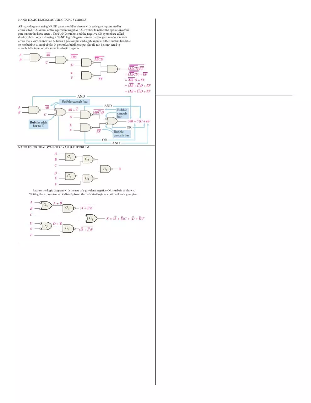
NAND LOGIC DIAGRAMS USING DUAL SYMBOLS
All logic diagrams using NAND gates should be drawn with each gate represented by
either a NAND symbol or the equivalent negative-OR symbol to reflect the operation of the
gate within the logic circuit. The NAND symbol and the negative-OR symbol are called
dual symbols. When drawing a NAND logic diagram, always use the gate symbols in such
a way that every connection between a gate output and a gate input is either bubble-tobubble
or nonbubble-to-nonbubble. In general, a bubble output should not be connected to
a nonbubble input or vice versa in a logic diagram.
NAND USING DUAL SYMBOLS EXAMPLE PROBLEM
Redraw the logic diagram with the use of equivalent negative-OR symbols as shown.
Writing the expression for X directly from the indicated logic operation of each gate gives:
Download Cheat Sheet 3
Cheat Sheet 3.pdf (PDF, 344.16 KB)
Download PDF
Share this file on social networks
Link to this page
Permanent link
Use the permanent link to the download page to share your document on Facebook, Twitter, LinkedIn, or directly with a contact by e-Mail, Messenger, Whatsapp, Line..
Short link
Use the short link to share your document on Twitter or by text message (SMS)
HTML Code
Copy the following HTML code to share your document on a Website or Blog
QR Code to this page

This file has been shared publicly by a user of PDF Archive.
Document ID: 0000309230.