PT2399 (PDF)
File information
Title: untitled
This PDF 1.5 document has been sent on pdf-archive.com on 02/03/2011 at 14:27, from IP address 98.244.x.x.
The current document download page has been viewed 3163 times.
File size: 354.87 KB (16 pages).
Privacy: public file


File preview
Tel: 886-2-66296288
Fax: 886-2-29174598
URL: http://www.princeton.com.tw
Echo Processor IC
PT2399
DESCRIPTION
PT2399 is an echo audio processor IC utilizing CMOS Technology which is equipped with ADC and
DAC, high sampling frequency and an internal memory of 44K Digital processing is used to generate
the delay time, it also features an internal VCO circuit in the system clock, thereby, making the frequency easily adjustable. PT2399 boast of very low distortion (THD<0.5%) and very low noise
(No<-90dBV), thus producing high quality audio output. The pin assignments and application circuit are
optimized for easy PCB layout and cost saving advantage.
FEATURES
•
•
•
•
•
•
•
CMOS Technology
Least External Components
Auto Reset Function
Low Noise, No<-90dBV Typical
Low Distortion, THD<0.5% Typical
External Adjustable VCO
Available in 16 pins, DIP or SOP
APPLICATIONS
•
•
•
•
•
•
•
•
Video Tape Recorder
Video Compact Disk
Television
CD Player
Car Stereo
KARAOKE Mixer
Electronic Musical Instrument
Audio Equipment with Echo Processor
PT2399 V1.4
-1-
October, 2005
Tel: 886-2-66296288
Fax: 886-2-29174598
URL: http://www.princeton.com.tw
Echo Processor IC
PT2399
10
4.7K
CC1
11
CC0
4.7K
OP1-OUT
13 12
OP1-IN
14
OP2-IN
LPF2-OUT
15
OP2-OUT
LPF1-OUT
16
LPF2-IN
LPF1-IN
BLOCK DIAGRAM
9
8
7
MOD
_
+
LPF1
+
LPF2
_
+
+
MO
DO1
CLOCK
MI
44K Bits
RAM
-2-
3
4
5
6
CLK_O
VCO
VCO
DGND
REF
PT2399 V1.4
DO0
AGND
VCC
AUTO
RESET
2
DEM
+
DI
1/2 Vcc
1
_
_
COMP
_
October, 2005
Tel: 886-2-66296288
Fax: 886-2-29174598
URL: http://www.princeton.com.tw
Echo Processor IC
PT2399
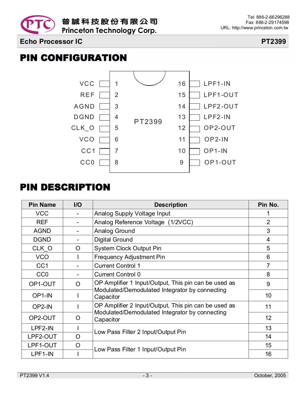
PIN CONFIGURATION
VCC
1
16
L P F1 -I N
REF
2
15
L P F1 -O U T
AGND
3
14
L P F2 -O U T
DGND
4
13
L P F2 -I N
C L K_ O
5
12
O P 2- O U T
VCO
6
11
O P 2- IN
CC1
7
10
O P 1- IN
CC0
8
9
P T2399
O P 1- O U T
PIN DESCRIPTION
Pin Name
VCC
REF
AGND
DGND
CLK_O
VCO
CC1
CC0
I/O
O
I
-
OP1-OUT
O
OP1-IN
I
OP2-IN
I
OP2-OUT
O
LPF2-IN
LPF2-OUT
LPF1-OUT
LPF1-IN
I
O
O
I
PT2399 V1.4
Description
Analog Supply Voltage Input
Analog Reference Voltage (1/2VCC)
Analog Ground
Digital Ground
System Clock Output Pin
Frequency Adjustment Pin
Current Control 1
Current Control 0
OP Amplifier 1 Input/Output, This pin can be used as
Modulated/Demodulated Integrator by connecting
Capacitor
OP Amplifier 2 Input/Output, This pin can be used as
Modulated/Demodulated Integrator by connecting
Capacitor
Low Pass Filter 2 Input/Output Pin
Low Pass Filter 1 Input/Output Pin
-3-
Pin No.
1
2
3
4
5
6
7
8
9
10
11
12
13
14
15
16
October, 2005
Tel: 886-2-66296288
Fax: 886-2-29174598
URL: http://www.princeton.com.tw
Echo Processor IC
PT2399
FUNCTION DESCRIPTION
ECHO MODE
Please refer to the diagram below:
Vout
Vin
+
Low P ass
Filter
Delay Time
Circuit
A /D
D/A
Low P ass
Filter
AUTO RESET FUNCTION
The waveform of the signal during power on is given below:
Power ON
Reset Time = 400 ms
PT2399 V1.4
-4-
October, 2005
Tel: 886-2-66296288
Fax: 886-2-29174598
URL: http://www.princeton.com.tw
Echo Processor IC
PT2399
ABSOLUTE MAXIMUM RATING
(Unless otherwise specified, Ta=25℃)
Parameter
Symbol
Supply Voltage
Vcc
Supply Current
Icc
Power Dissipation
Pd
Operation Temperature
Topr
Storage Temperature
Tstg
Rating
6.5
100
1.7
-40 to +85
-65 to +150
Unit
V
mA
W
℃
℃
RECOMMENDED OPERATING CONDITIONS
Parameter
Supply Voltage
Clock Frequency
Symbol
Vcc
fck
Min.
4.5
-
Typ.
5
4
Max.
5.5
5
Unit
V
MHz
AC CHARACTERISTICS
(Unless otherwise specified: Vcc=5.0V, fin=1KHz, Vi=100mVrms, fck=2MHz, Ta=25℃)
Parameter
Symbol
Test Condition
Min.
Typ.
Supply Voltage
Vcc
4.5
5.0
Supply Current
Icc
30
Voltage Gain
Gv
RL=47KΩ
-0.5
Max. Output Voltage
Vomax
THD=10%
1.5
2
Output Distortion
THD
filter=A-weighting
0.3
Output Noise Voltage
No
filter=A-weighting
-90
Power Supply Rejection
ΔVcc=-20dBV(0.1Vrms),
PSRR
-40
Ratio
f=100Hz
PT2399 V1.4
-5-
Max.
5.5
40
2.5
2.5
1.0
-80
Unit
V
mA
dB
Vrms
%
dBV
-30
dB
October, 2005
Tel: 886-2-66296288
Fax: 886-2-29174598
URL: http://www.princeton.com.tw
Echo Processor IC
PT2399
APPLICATION CIRCUIT
ECHO
4.7 µF
15K
3900pF
Input
+
100K
+5V
0.1 µF
+
100 µF
47 µF
+
1
16
2
15
3
14
4
13
5
20K
0.1 µF
R
6
PT23 99
4.7 µF
10K
560pF
+
10K
10 µF
+
0.01µ F
50K
560pF
11
10
8
9
10K
Output
+
15K
12
7
10 µF
4.7K
5.6K
0.082 µF
10K
3300pF
10K
0.082 µF
AGND
DGND
0.1 µF
Note:
External Resistor having a value of 10 KΩ to 50 KΩ may be used. The recommended Resistor Value(R)
is 10 KΩ. When the value of the Resistor (R) increases, the range of the Delay Time also increases.
PT2399 V1.4
-6-
October, 2005
Tel: 886-2-66296288
Fax: 886-2-29174598
URL: http://www.princeton.com.tw
Echo Processor IC
PT2399
SURROUND/DELAY
15K
5600pF
4.7 µF
Input
100K
+5V
0.1 µF
100 µF
47 µF
1
16
2
15
3
14
4
5
R
0.1 µF
PT23 99
560pF
15K
2.7K
10 µF
15K
12
11
7
10
Output
0.01µ F
13
6
8
10K
560pF
0.1 µF
9
10K
5600pF
15K
0.1 µF
AGND
DGND
0.1 µF
Note: Please refer to Table 1 for the Resistor/Delay Time values.
PT2399 V1.4
-7-
October, 2005
Tel: 886-2-66296288
Fax: 886-2-29174598
URL: http://www.princeton.com.tw
Echo Processor IC
PT2399
TABLE 1: RESISTOR/DELAY TIME VALUES
R
fck
td
THD
27.6K
2.0M
342ms
1.0%
21.3K
2.5M
273ms
0.8%
17.2K
3.0M
228ms
0.63%
14.3K
3.5M
196ms
0.53%
12.1K
4.0M
171ms
0.46%
10.5K
4.5M
151ms
0.41%
9.2K
5.0M
136.6ms
0.36%
8.2K
5.5M
124.1ms
0.33%
R
fck
td
THD
7.2K
6.0M
113.7ms
0.29%
6.4K
6.5M
104.3ms
0.27%
5.8K
7.0M
97.1ms
0.25%
5.4K
7.5M
92.2ms
0.25%
4.9K
8.0M
86.3ms
0.23%
4.5K
8.5M
81ms
0.22%
4K
9.0M
75.9ms
0.21%
3.4K
10M
68.1ms
0.19%
R
fck
td
THD
2.8K
11M
61.6ms
0.18%
2.4K
12M
56.6ms
0.16%
2K
13M
52.3ms
0.15%
1.67K
14M
48.1ms
0.15%
1.47K
15M
45.8ms
0.15%
1.28K
16M
43ms
0.15%
1.08K
17M
40.6ms
0.14%
894
18M
38.5ms
0.14%
R
fck
td
THD
723
19M
36.6ms
0.14%
519
20M
34.4ms
0.13%
288
21M
32.6ms
0.13%
0.5
22M
31.3ms
0.13%
Note:
1. R = External Resistor (Ω), please refer to PT2399 Surround/Delay Time Application Circuit.
2. fck = Clock Frequency (Hz).
3. td = Delay Time
4. THD = Total Harmonic Distortion
PT2399 V1.4
-8-
October, 2005
Tel: 886-2-66296288
Fax: 886-2-29174598
URL: http://www.princeton.com.tw
Echo Processor IC
PT2399
ORDER INFORMATION
Part Number
PT2399
PT2399S
PT2399-SN
PT2399 (L)
PT2399S (L)
PT2399-SN (L)
Package Type
16 Pins, DIP, 300mil
16 Pins, SOP, 300mil
16 Pins, SOP, 150mil
16 Pins, DIP, 300mil
16 Pins, SOP, 300mil
16 Pins, SOP, 150mil
Top Code
PT2399
PT2399S
PT2399-SN
PT2399
PT2399S
PT2399-SN
Notes:
1. (L), (C) or (S) = Lead Free.
2. The Lead Free mark is put in front of the date code.
PT2399 V1.4
-9-
October, 2005
Tel: 886-2-66296288
Fax: 886-2-29174598
URL: http://www.princeton.com.tw
Echo Processor IC
PT2399
PACKAGE INFORMATION
16 PINS, DIP, 300 MIL
PT2399 V1.4
- 10 -
October, 2005
Tel: 886-2-66296288
Fax: 886-2-29174598
URL: http://www.princeton.com.tw
Echo Processor IC
PT2399
Symbol
A
A1
A2
b
b1
b2
b3
c
c1
D
D1
E
E1
e
eA
eB
eC
L
Min.
0.015
0.115
0.014
0.014
0.045
0.030
0.008
0.008
0.780
0.005
0.300
0.240
0.000
0.115
Nom.
0.130
0.018
0.018
0.060
0.039
0.010
0.010
0.790
0.310
0.250
0.100 BSC.
0.300 BSC.
0.130
Max.
0.210
0.195
0.022
0.020
0.070
0.045
0.014
0.011
0.800
0.325
0.280
0.430
0.060
0.150
Notes:
1.
Controlling Dimension: INCHES.
2.
Dimensioning and tolerancing per ANSI Y14.5M-1982.
3.
Dimensions “A”, “A1” and “L” are measured with the package seated in JEDEC Seating Plane
Gauge GS-3.
4.
“D, “D1” and “E1” dimensions do not include mold flash or protrusions. Mold flash or protrusions
shall not exceed 0.010 inch.
5.
“E” and “eA” measured with the leads constrained to be perpendicular to datum -C-.
6.
“eB” and “eA” are measured at the lead tips with the leads unconstrained.
7.
N is the maximum number of terminal positions (N=16).
8.
Pointed or rounded lead tips are preferred to ease insertion.
9.
“b2” and “b3” maximum dimensions do not include dambar protrusions. Dambar protrusions shall
not exceed 0.010 (0.25mm).
10. Variation AB is a full lead package.
11. Distance between leads including dambar protrusions to be 0.005 in minimum.
12. Datum plane -H- coincident with the bottom of lead where lead exits body.
13. Refer to JEDEC MS-001 Variation AB.
JEDEC is the registered trademark of JEDEC SOLID STATE TECHNOLOGY ASSOCIATION.
PT2399 V1.4
- 11 -
October, 2005
Tel: 886-2-66296288
Fax: 886-2-29174598
URL: http://www.princeton.com.tw
Echo Processor IC
PT2399
16 PINS, SOP, 300 MIL
Symbol
A
A1
B
C
D
E
e
H
h
L
α
PT2399 V1.4
Min.
Max
2.35
2.65
0.10
0.30
0.33
0.51
0.23
0.32
10.10
10.50
7.40
7.60
1.27 BSC.
10.00
10.65
0.25
0.75
0.40
1.27
0o
8o
- 12 -
October, 2005
Tel: 886-2-66296288
Fax: 886-2-29174598
URL: http://www.princeton.com.tw
Echo Processor IC
PT2399
Notes:
1. Controlling Dimension: MILLIMETER
2. Dimensioning and tolerancing per ANSI Y14.5M-1982.
3. Dimension “D” does not include mold flash, protrusions or gate burrs. Mold flash, protrusions and
gate burrs shall not exceed 0.15mm (0.006 in) per side.
4. Dimension “E” does not include interlead flash or protrusions. Interlead flash and protrusions shall
not exceed 0.25 mm (0.010 in.) per side
5.. The chamfer on the body is optional. If it is not present, a visual index feature must be located
within the crosshatched area
6. L is the length of the terminal for soldering to a substrate.
7. N is the number of terminal positions (N=16).
8
The lead width B, as measured 0.36 mm (0.014in) or greater above the seating plane, shall not
exceed a maximum value of 0.61mm (0.024in.)
9. Refer to JEDEC MS-013 Variation AA.
JEDEC is the registered trademark of JEDEC SOLID STATE TECHNOLOGY ASSOCIATION.
PT2399 V1.4
- 13 -
October, 2005
Tel: 886-2-66296288
Fax: 886-2-29174598
URL: http://www.princeton.com.tw
Echo Processor IC
PT2399
16 PINS, SOP, 150MIL
PT2399 V1.4
- 14 -
October, 2005
Tel: 886-2-66296288
Fax: 886-2-29174598
URL: http://www.princeton.com.tw
Echo Processor IC
PT2399 V1.4
PT2399
- 15 -
October, 2005
Tel: 886-2-66296288
Fax: 886-2-29174598
URL: http://www.princeton.com.tw
Echo Processor IC
Symbol
A
A1
A2
b
b1
c
c1
D
E
E1
e
L
L1
L2
R
R1
h
θ
θ1
θ2
PT2399
Min.
1.35
0.10
1.25
0.31
0.28
0.17
0.17
0.40
0.07
0.07
0.25
0°
5°
0°
Typ.
9.90 BSC.
6.00 BSC.
3.90 BSC.
1.27 BSC.
1.04 REF.
0.25 BSC.
-
Max.
1.75
0.25
1.65
0.51
0.48
0.25
0.23
1.27
0.50
8°
15°
-
Note:
1.
Dimensioning and tolerancing per ANSI Y 14.5M-1994
2.
Controlling Dimension: MILLIMETERS.
3.
Dimension D does not include mold flash protrusions or gate burrs. Mold flash, protrusions or
gate burrs shall not exceed 0.15 mm (0.006 in) per end. Dimension E1 does not include
interlead flash or protrusion. Interlead flash or protrusion shall not exceed 0.25mm per side. D
and E1 dimensions are determined at datum H.
4.
The package top may be smaller than the package bottom. Dimensions D and E1 are
determined at the outermost extremes of the plastic body exclusive of mold flash, tie bar burrs,
gate burrs and interlead flash, but including any mismatch between the top and bottom of the
plastic body.
5.
Datums A & B to be determined at datum H.
6.
N is the number of terminal positions. (N=16)
7.
The dimensions apply to the flat section of the lead between 0.10 to 0.25mm from the lead tip.
8.
Dimension “b” does not include dambar protrusion. Allowable dambar protrusion shall be
0.10mm total in excess of the “b” dimension at maximum material condition. The dambar cannot
be located on the lower radius of the foot.
9.
This chamfer feature is optional. If it is not present, then a pin 1 identifier must be located within
the index area indicated.
10. Refer to JEDEC MS-012, Variation AC.
JEDEC is the registered trademark of JEDEC SOLID STATE TECHNOLOGY ASSOCIATION.
PT2399 V1.4
- 16 -
October, 2005
Download PT2399
PT2399.pdf (PDF, 354.87 KB)
Download PDF
Share this file on social networks
Link to this page
Permanent link
Use the permanent link to the download page to share your document on Facebook, Twitter, LinkedIn, or directly with a contact by e-Mail, Messenger, Whatsapp, Line..
Short link
Use the short link to share your document on Twitter or by text message (SMS)
HTML Code
Copy the following HTML code to share your document on a Website or Blog
QR Code to this page

This file has been shared publicly by a user of PDF Archive.
Document ID: 0000028887.