10 10Nov15 547 1059 1 ED (PDF)
File information
Title: Microsoft Word - 10 10Nov15 547-1059-1-ED
Author: TH Sutikno
This PDF 1.5 document has been generated by PScript5.dll Version 5.2.2 / Acrobat Distiller 10.0.0 (Windows), and has been sent on pdf-archive.com on 25/09/2016 at 06:03, from IP address 36.73.x.x.
The current document download page has been viewed 308 times.
File size: 239.48 KB (4 pages).
Privacy: public file


File preview
Bulletin of Electrical Engineering and Informatics
ISSN: 2302-9285
Vol. 5, No. 1, March 2016, pp. 88~91, DOI: 10.11591/eei.v5i1.547
88
Organic Thin Film Transistor with Carbon
Nanotube Electrodes
1,2
Kianoosh Safari*1, Ali Rafiee2, Hamidreza-Dalili-Oskouei3
Department Of Electrical and Electronic Engineering, Islamic AzadUniversity, Bushehr Branch, Bushehr,
Iran
3
University of Aeronautical Science & Technology, Tehran, Iran
*Corresponding author, e-mail: safari.kianoosh@yahoo.com
Abstract
The contact resistance between organic semiconductors and metallic electrodesaffectsthe
performance of the organic thin film transistor (OTFT) negatively so that it may make thefield effect mobility
of charge carrier seem small. In order to reduce the contact resistance weused conducting Carbon
Nanotube (CNT) films, which consist of the same element as the basicmaterial of the organic
semiconductors, as source or drain electrodes. The measurements oftransistor properties based on
pentacene single crystals have been carried out by using both CNTfilm electrodes and metal electrodes.
Keywords: Organic transistor, carbon nanotube, electrical characteristic
1. Introduction
Finding good semiconducting organic materials is the first step for the high performance
Organic Thin Film Transistor (OTFT), and some organic materials, like pentacene or rubrene,
have already been found to be good candidates which could substitute the inorganic
semiconductor [1, 2]. However, there are still difficulties to make application to the electronic
device due to several factors, the incomplete understanding of the charge transport mechanism,
the contact effects between the metallic electrodes and the organic active materials, the
imperfection of the organic active layer- the insulating layer interface etc [3-5]. The contact
barrier sometimes limits the charge carrier transport of the OTFT or gating effect, which results
in Non-linear IV characteristics or the degradation of charge carrier’s field effect mobility [4, 6].
Furthermore, it is unclear to distinguish between the intrinsic material property and the extrinsic
deterioration caused by the contact regime. So, the technique to reduce the contact resistance
is also an important part of the OTFT experiment in order to understand the essential nature of
carriers in organic semiconductors, and to make applications of electronic devices [7-12].
We have recently fabricated TFT structure using anthracene single crystals in orderto
study the grain boundary-free properties of the charge carrier transport [5]. In that TFTstructure
the plate-shaped anthracene single crystal was put on the pre-patterned metalelectrodes of the
SiO2/Si substrate, and then it was pressed down. The results showedthat the high contact
resistance could be reduced by chemical treatment for the metalelectrodes. This means that
charge injection was enhanced by the chemical reatment, i.e. modifying the electrode-surfacematerials. Graciela B. Blanchet et.al. also showedthat non-metallic electrodes, namely printed
organic conducting electrodes, couldreduce the contact resistance [4]. In this paper we will
present the properties of pentacene single crystal Thin Film Transistor with the conducting CNT
film electrodes and compare with the result of metal electrode TFT.
Received September 9, 2015; Revised November 23, 2015; Accepted December 16, 2015
89
ISSN: 2089-3191
Figure 1. Schematic of crystal growth apparatus: (a) temperature profiles of quartz tube furnace
and (b) Pentacene single crystal grown by physical vapor deposition method [8].
Figure 1. Schematic diagram of electrodes fabrication with different SWCNT densities.
(i) Assembly of the aligned array SWCNTs by dielectrophoresis (DEP) between the Pd
electrodes. (ii) SWNCT assembly with different densities, which were controlled by tuning the
SWCNT solution concentration (iii) Opened a window on the SWCNTs array via electron beam
lithography and (iv) Etch the SWCNTs by oxygen plasma.
2. Experimental Details
Commercial pentacene powder purchased from Aldrich was used to grow a single
crystal in a quartz tube furnace, 65cm long, which shows temperature gradient of~100°C
between the middle and the edge, as shown in Figure 1 (a). The crystals appeared at the
200~220°C temperature region after several hours keeping the temperature of the source zone
at 300°C under slow nitrogen gas flow (20ml/min). Figure 1 (b) shows pentacene single crystals
which are in the shape of plates with 2~5mm size. These palate-shaped crystals were put on
CNT electrodes prepared as in Figure 2 (a).
Figure 2. Procedure of the CNT electrodes fabrication on the Si/SiO2 substrates (a), AFM image
of the metal based CNT electrodes (b).
Bulletin of EEI Vol. 5, No. 1, March 2016 : 88 – 91
Bulletin of EEI
ISSN: 2302-9285
90
The heavily doped Si substrate with SiO2 layer 200nm thick was prepared to beused as
gate electrode and gate insulating layer. Optical lithography allows to makephoto resist masks
of 5, 30, 50 μm channel length, shadowing metal evaporation andCNT film coating. After the
evaporations of Cr 3nm thick and AuPd 17nm thick, CNTfilm was deposited by air-brushing
CNT suspensions in chloroform, DMF and SDS solutions respectively, in which the chloroform
suspension gave the best results. Whena dense CNT layer was deposited, it was difficult to get
a clear electrode edge because the randomly entangled CNT have a tendency to prevent photo
resist lift-off. Figure 2(b) shows the AFM image of CNT electrodes based on metal of 5 μm
channel length. As shown in Figure 2 (b) CNT passed cross the electrode edge, but it is small
enoughto be neglected compared with the whole channel length, 5 μm. TFT structures were
fabricated by combining pentacen single crystals and the CNTelectrodes. Pressure was applied
to enhance the contact between pentacene and CNT like in our previous works5. We measured
field effect characteristics of 5, 30, 50 μm channel lengths CNT electrodes and metal
electrodes, respectively, at room temperature after checking negligible the gate leakage current
less than 10-11.
3. Results and Discussions
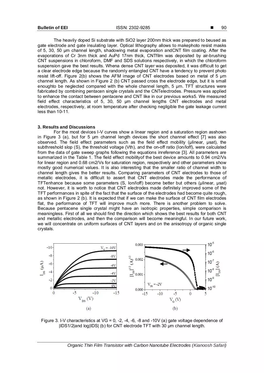
For the most devices I-V curves show a linear region and a saturation region asshown
in Figure 3 (a), but for 5 μm channel length devices the short channel effect [7] was also
observed. The field effect parameters such as the field effect mobility (μlinear, μsat), the
subthreshold slop (S), the threshold voltage (Vth), and the on-off ratio (Ion/Ioff), were calculated
from the data of gate sweep graphs following the equations inreference [3]. All parameters are
summarized in the Table 1. The field effect mobilityof the best device amounts to 0.94 cm2/Vs
for linear region and 0.68 cm2/Vs for saturation region, respectively and other parameters show
mostly good numerical values. It is also interesting that the smaller ratio of channel width to
channel length gives the better results. Comparing parameters of CNT electrodes to those of
metallic electrodes, it is difficult to assert that CNT electrodes made the performance of
TFTenhance because some parameters (S, Ion/Ioff) become better but others (μlinear, μsat)
not. However, it is worth to notice that CNT electrodes made definitely improved some of the
TFT performances in spite of the fact that the surface of the electrodes had become quite rough,
as shown in Figure 2 (b). It is expected that if we can make the surface of CNT film electrodes
flat, the performance of TFT will improve much more. There is another problem to solve.
Because pentacene single crystal might have an isotropic properties, simple comparison is
meaningless. First of all we should find the direction which shows the best results for both CNT
and metallic electrodes, and then the comparison will become meaningful. In our future work,
we will concentrate on uniform surfaces of CNT layers and on the anisotropy of organic single
crystals.
Figure 3. I-V characteristics at VG = 0, -2, -4, -6, -8 and -10V (a) gate voltage dependence of
|IDS1/2|and log|IDS| (b) for CNT electrode TFT with 30 μm channel length.
Organic Thin Film Transistor with Carbon Nanotube Electrodes (Kianoosh Safari)
91
ISSN: 2089-3191
Table 1. Feld effect parameters where W/L is the ratio of channel width to channel length
References
[1] SF Nelson, YY Lin, DJ Gundlach, and TN Jackson. Appl. Phys. Lett. 1998; 72: 1854-1856.
[2] VC Sundar, J Zaumseil, V Pozdrov, E Menard, R Willett, T Someya, ME Gershenson, and JA Rogers.
Science. 2004; 303: 1644-1646.
[3] G Horowitz. Adv. Mater. 1998; 10: 365-377.
[4] GB Blanchet, CR Fincher, M Lefenfeld, and LA Rogers. Appl. Phys. Lett. 2004; 84: 296-298.
[5] AN Aleshin, JY Lee, SW Chu, JS Kim, and YW Park. Appl. Phys. Lett. 2004; 84: 5383-5385.
[6] AN Aleshin, SW Chu, VI Kozub, SW Lee, JY Lee, SH Lee, DW Kim and YW Park. Curr. Appl. Phys.
2005; 5: 85-89.
[7] MD Jacunski, MS Shur, AAA Owusu, T Ytterdal, M Hack, and B Iniguez. IEEE Trans. Electron Dev.
1999; 46: 1146- 1158.
[8] RA Aaudise, Ch Kloc, PG Simpkins, and T Siegrist. J. Crys. Growth. 1998; 187: 449-454.
[9] Koch N, Kahn A, Ghijsen J, Pireaux JJ, Schwartz J, Johnson RL and Elschner A. Conjugated organic
molecules on metal versus polymer electrodes: demonstration of a key energy level alignment
mechanism. Appl. Phys. Lett. 2003; 82: 70-2.
[10] Qi P, Javey A, Rolandi M, Wang Q, Yenilmez E and Dai H. Miniature organic transistors with carbon
nanotubes as quasi-one-dimensional electrodes. J. Am. Chem. Soc. 2004; 126: 11774-5.
[11] Aguirre CM, Ternon C, Paillet M, Desjardins P and Martel R. Carbon nanotubes as injection
electrodes for organic thin film transistors. Nano Lett. 2009; 9: 1457-61.
[12] Hellstrom SL, Jin RZ, Stoltenberg RM and Bao Z. Driving high-performance n- and p-type organic
transistors with carbon nanotube/conjugated polymer composite electrodes patterned directly from
solution. Adv. Mater. 2010; 22: 4204-8.
Bulletin of EEI Vol. 5, No. 1, March 2016 : 88 – 91
Download 10 10Nov15 547-1059-1-ED
10 10Nov15 547-1059-1-ED.pdf (PDF, 239.48 KB)
Download PDF
Share this file on social networks
Link to this page
Permanent link
Use the permanent link to the download page to share your document on Facebook, Twitter, LinkedIn, or directly with a contact by e-Mail, Messenger, Whatsapp, Line..
Short link
Use the short link to share your document on Twitter or by text message (SMS)
HTML Code
Copy the following HTML code to share your document on a Website or Blog
QR Code to this page

This file has been shared publicly by a user of PDF Archive.
Document ID: 0000486780.