1338 Bowers IPC 2013 (PDF)
File information
Title: Bowers_IPC 2013.pptx
Author: John Bowers
This PDF 1.3 document has been generated by PowerPoint / Mac OS X 10.9.1 Quartz PDFContext, and has been sent on pdf-archive.com on 01/03/2017 at 18:52, from IP address 38.122.x.x.
The current document download page has been viewed 455 times.
File size: 12.79 MB (37 pages).
Privacy: public file


File preview
Integration of Active Elements onto Low
Loss Waveguides for Silicon Interposers
John Bowers
Director, Institute for Energy Efficiency
Kavli Professor of Nanotechnology
Departments of Materials and Electrical and Computer Engineering
University of California, Santa Barbara
bowers@ece.ucsb.edu
http://optoelectronics.ece.ucsb.edu/
UCSB: Jared Bauters, Jock Bovington, Daryl Spencer,
Molly Piels, Mike Davenport and Martijn Heck
Intel : Richard Jones, Mario Paniccia, Matt Sysak
Aurrion: Alex Fang, Greg Fish, Eric Hall, Brian Koch
Research at UCSB supported by Jag Shah and Josh Conway at DARPA MTO, Intel, Aurrion and HP
1
Outline
• 2.5D Integration using Silicon Interposers: Why
Photonics? Why Silicon Photonics?
• Hybrid Silicon photonic devices
• Low loss Silicon nitride waveguides
• Integration of Low loss waveguides with hybrid
silicon photodetectors
• Silicon Photonic Integrated Circuits
2
Why Photonic Interconnects for Interposers?
2.5D Integration
• Electrons are charged particles. They are fermions. Electronic crosstalk
is inherent.
• Photons are bosons. They don’t interact (you have to work hard to do
so). Crosstalk is minimal. 50 Tbps on a waveguide is possible.
• For short lengths, power to drive an electrical connection is proportional
to its length.
• Power to drive an optical connection is the same for 1 micron to 100 km.
3
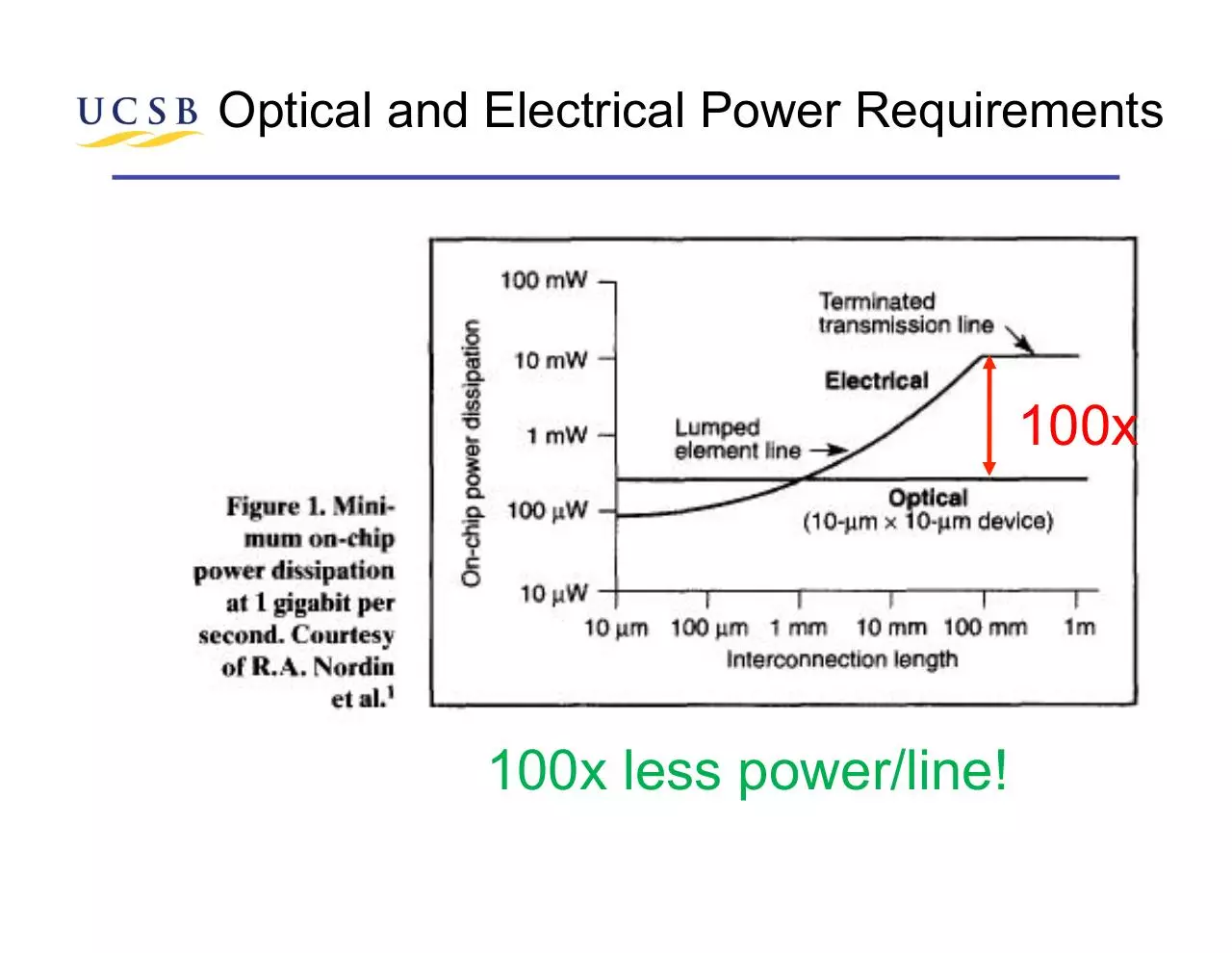
Optical and Electrical Power Requirements
100x
100x less power/line!
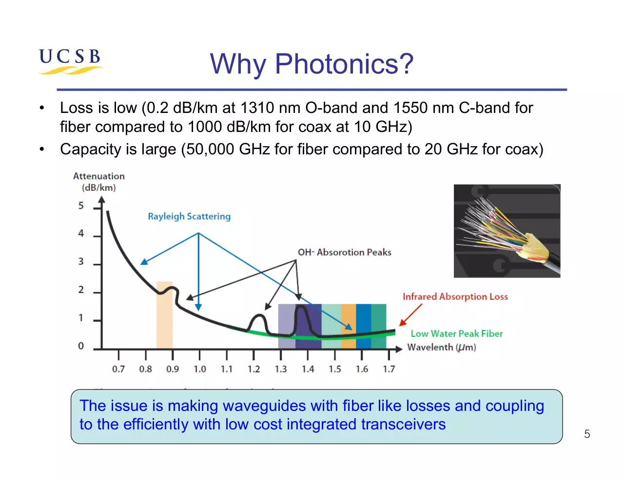
Why Photonics?
• Loss is low (0.2 dB/km at 1310 nm O-band and 1550 nm C-band for
fiber compared to 1000 dB/km for coax at 10 GHz)
• Capacity is large (50,000 GHz for fiber compared to 20 GHz for coax)
The issue is making waveguides with fiber like losses and coupling
to the efficiently with low cost integrated transceivers
5
Why Silicon Photonics?
• Integrate photonics with electronics
– Same wafer
– Bump bonding of silicon PIC with silicon IC
• Same coefficient of thermal expansion
– 3D stacking
Cross-sectional view of an IBM Silicon
Nanophotonics chip combining optical and
electrical circuits
Vlasov et al. IEDM postdeadline
• Reduce cost by going to larger diameter wafers
– InP limited by wafer breakage to 100 mm diameter
• Reduce cost by sharing VLSI facility with electronics
• Improve yield by taking advantage of silicon process
development
• Volume driver: Solve IC interconnect bottleneck (from 4
Tbps to 1 Pbps). Optical transmitters/receivers on
processors, memories, switches.
6
Moving to Interconnects
Optical
Copper
Chip to Chip
Metro &
Long Haul
0.1 – 80 km
Intel
Optical
Products
1 – 50 cm
Billions
50 – 100 cm
Rack to
Rack
Volumes
Board to Board
Millions
1 to 100 m
Thousands
Decreasing Distances!
Drive optical to high
volumes and low costs
7
Evolution of Optical Transceivers
On Face Plate
On-board
In-Package
Aurrion
JDSU
Avago
Density ↑
Power ↓
Cost ↓
Xilinx/Luxtera
8
In Package: Required Technology
Fraunhofer
Electronic Packaging and Assembly
Techniques
Low Cost Optical
Connectors
Alex Fang Today 1:30 pm
ME 3.1 Evergreen B
Complete Photonic Integration
20C
80C
Uncooled WDM Laser
Arrays
>25Gb/s Modulators &
Photodiodes
Low Loss
Passives
Download 1338 Bowers IPC 2013
1338_Bowers_IPC 2013.pdf (PDF, 12.79 MB)
Download PDF
Share this file on social networks
Link to this page
Permanent link
Use the permanent link to the download page to share your document on Facebook, Twitter, LinkedIn, or directly with a contact by e-Mail, Messenger, Whatsapp, Line..
Short link
Use the short link to share your document on Twitter or by text message (SMS)
HTML Code
Copy the following HTML code to share your document on a Website or Blog
QR Code to this page

This file has been shared publicly by a user of PDF Archive.
Document ID: 0000562435.